


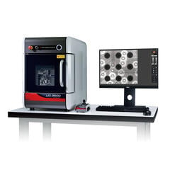
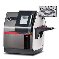
In semiconductor manufacturing, X-ray inspection is used to examine the state of wire bonding at high magnification, checking for issues such as wire breakage, pitch deviation, and poor bonding.
Once sealed with resin molding, IC chip wire bonding cannot be inspected visually. Furthermore, the wires have a fine structure of approximately 20 to 30 μm. Therefore, a high-resolution X-ray system is required for effective inspection.
Inspecting for wire breakage, poor bonding, and wire sweep requires X-ray imaging that remains clear even at high magnification. To achieve this, the X-ray inspection system must allow for a small focal spot size.
Matsusada Precision's X-ray inspection systems feature proprietary microfocus X-ray tubes. Leveraging our expertise in high-voltage power supplies, we have achieved industry-leading focal spot sizes of 5 μm for benchtop systems and 4 μm for stationary systems, ensuring clear observation. With advanced CT technology, we also offer 2D and 3D CT scan functions designed to inspect wire bonding for three-dimensional shape and delamination.
Additionally, X-ray inspection is effective for authenticating semiconductor IC chips and detecting counterfeits.

| Focal spot | Microfocus |
|---|---|
| X-ray tube voltage | 90 kV |
| Magnification | 100x or more |
Recommended products


Related Technical Articles
- Back-End Semiconductor Manufacturing Process
- Selecting an X-ray Inspection System
- Principles of Radiography
- Safe Operation of X-ray Inspection Systems
- What is Microfocus X-ray Technology? (Basic Knowledge)
- Basics and Principles of Computed Tomography (CT)
- Non-Destructive Testing: Types and Applications
- What are X-rays? (Basic Knowledge)
- How to Acquire High-Quality Computed Tomography (CT) Images - X-ray NDT series (1)
- A Guide to X-ray CT Images: Formats, Viewing, and Applications - X-ray NDT series (2)
- X-ray Image Processing and Automated Inspection - X-ray NDT series (3)
- Types of X-ray Tubes and High-voltage Power Supplies
- What is the difference between Radioactivity, Radiation, and Radioactive Materials?
- Understanding Radiation: Effects on the Body and X-ray Safety