Front-end and back-end processes
The process of manufacturing semiconductors is similar to creating business cards.
In the case of business cards, the first step is to finalize a design, followed by printing several copies on a large sheet of paper. Finally, the printed sheet is cut to produce individual cards.
The semiconductor manufacturing process follows a similar workflow. Manufacturing is divided into design, front-end, and back-end processes. The design process corresponds to the card design, and the front-end process corresponds to printing. The subsequent step involves cutting the wafers into individual pieces.
Semiconductors undergo a design process, and large-scale integrated circuits (LSI) are created on silicon wafers during the front-end process. These integrated circuits are then cut into individual chips during the back-end process. This article discusses the back-end process.
Outline of back-end process
In the back-end process, the semiconductor is cut from the wafer and packaged into a final product. While the front-end process creates large-scale integrated (LSI) circuits on a silicon wafer, the back-end process separates these circuits and processes them for use in electronic devices.
The key steps in back-end processing are as follows:
-
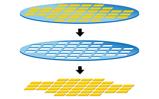
Dicing: The wafer is cut with a diamond blade and separated into individual chips. During the dicing process, the wafer is attached to dicing tape. A rotating circular diamond blade separates the semiconductors while ultrapure water is sprayed to cool the blade and remove debris.
In addition to the diamond blade method, other dicing techniques exist, such as laser dicing, the scribe method (creating cracks by scratching the surface), and plasma dicing (using plasma etching for separation).
When dicing tape is used, the tape holding the wafer must remain intact. After cutting, the dicing tape is stretched to create clearance between the chips, facilitating their removal.
-
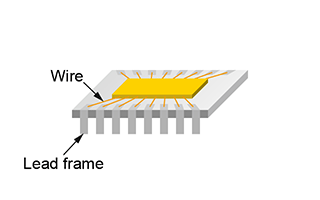
Wire bonding: The chip is mounted onto a lead frame (die bonding). A lead frame is a thin metal structure that supports the chip and serves as the terminal for connecting the semiconductor to a circuit board.
For power semiconductors or applications requiring high heat dissipation, chips may be mounted directly onto heat sinks. Adhesives such as silver paste are typically used for die bonding.
Following die bonding, the wire-bonding process connects the chip to the lead frame using thin gold wires, establishing the electrical connection.
-
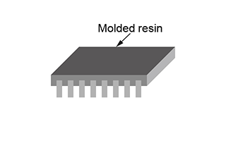
Molding: Semiconductor chips are delicate and easily damaged by scratches, shock, dust, and magnetism. To protect them from these external factors, the chip is encased in epoxy resin. This process is called molding or packaging.
However, recent trends toward device miniaturization have increased the demand for smaller semiconductors. One solution is the use of "bare dies"--semiconductors that are used without traditional packaging. While bare dies allow for high-density, 3D stacking on substrates, they require careful handling.
After dicing, wire bonding, and molding, semiconductor products undergo rigorous inspection before shipment.
Matsusada Precision Technology in Back-End Process
-
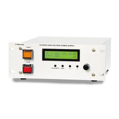
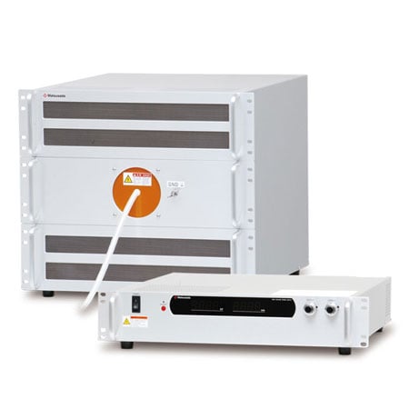
Dicing: Wafer cutting requires exceptional precision. Matsusada Precision's high-performance high-voltage power supplies are used to ensure stability in various cutting technologies. In plasma dicing, electrostatic chucks are used to secure the wafer, requiring specialized high-voltage power supplies to generate the clamping force.
-
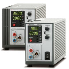
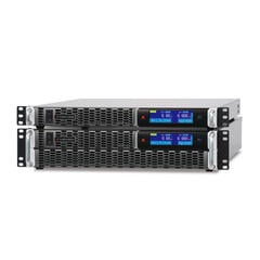
Wire bonding: Lead frames used in wire bonding undergo electroplating to improve conductivity and bonding reliability. In this process, the metal frame is immersed in a plating solution, and an electric current is applied to deposit metal onto the surface. Matsusada Precision provides precise DC power supplies essential for this electroplating process.
-
Evaluation testing: The pre-shipment inspection process includes dielectric breakdown testing, electrostatic discharge (ESD) testing, and non-destructive X-ray inspection. In dielectric breakdown testing, high voltage is applied to the insulator covering the semiconductor to measure the voltage limit at which the insulation fails.
To assess durability against static electricity from human touch, ESD testing is performed. During this test, a capacitor is charged to a high voltage and then discharged rapidly to simulate a static pulse. Matsusada Precision offers high-voltage power supplies optimized for both dielectric breakdown and ESD testing systems.
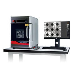
For internal quality checks, non-destructive X-ray inspection allows operators to verify the internal state of a sealed package. Matsusada Precision offers a lineup of X-ray inspection systems designed specifically for high-resolution semiconductor analysis.
Reference (Japanese site)
- 日立ハイテク - 半導体製造工程
(https://www.hitachi-hightech.com/jp/products/device/semiconductor/process.html) - SEMI - イラストで分かる半導体製造工程
(https://www.semijapanwfd.org/manufacturing_process.html) - TEL(東京エレクトロン株式会社) - 半導体ができるまで - Process
(https://www.tel.co.jp/museum/exhibition/process/process7.html)
Recommended products
Matsusada Precision's products meet the stringent specifications required by semiconductor manufacturing processes and are used throughout the fabrication process.