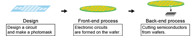
Overview of Semiconductor Manufacturing Process
The semiconductor manufacturing process is generally divided into three main phases: design, front-end processing, and back-end processing. The tasks performed in each stage are as follows:
- Design process: Engineers design the circuit patterns. This phase also involves creating photomasks for each layer of the circuit, which serve as blueprints for the lithography process.
- Front-end process: Multiple integrated circuits (ICs) are fabricated on a silicon wafer. This involves creating transistors and wiring layers.
- Back-end process: The wafer is diced to separate individual chips. These chips are then mounted, bonded, and encapsulated in resin to complete the final product.
Processing performed in the front-end process
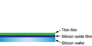
In the front-end process, circuits are formed on the surface of the silicon wafer. Wafers are thin slices of cylindrical silicon ingots with diameters ranging from 50 mm to 300 mm. On the surface of a wafer, dozens to hundreds of dies (or chips) with the same circuit are formed in a lattice-like arrangement.
The transistor layer is formed at the lowest level of the wafer surface. Semiconductors are made by forming many layers of wiring circuit layers on top of a transistor layer. In the transistor and wiring circuit layers, the three processes of film deposition, pattern transfer, and etching are repeated. The following is a description of the processing that takes place in each process.
-
Thin-film deposition: Thin films are formed on wafers to serve as materials for wiring and transistors. At this stage, the films do not yet contain circuit patterns. Deposition is primarily performed using PVD (Physical Vapor Deposition) or plasma CVD techniques.
Sputtering (PVD): Sputtering uses electrical discharge to generate plasma ions that bombard a target material. The impact ejects atoms from the target, which then settle on the wafer surface to form a thin film.
Vacuum Deposition (PVD): In vacuum deposition, an electron beam irradiates the source material in a vacuum, causing it to evaporate. The vapor then condenses on the wafer surface.
Plasma CVD: In plasma CVD, source gases are introduced above the substrate and converted into reactive plasma using electric fields or microwaves. Chemical reactions within the plasma deposit the desired material onto the wafer.
-
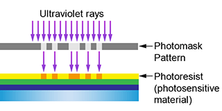
Lithography: This is the process of selecting the portions of the thin film formed by deposition that will remain as circuit patterns and those that will no longer be needed. A photoresist (photosensitive agent) is applied to the thin film, which is then irradiated with UV light through a photomask pattern. The pattern is then developed on the photosensitive material.
-
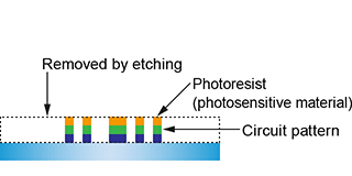
Etching: This is the process of removing specific areas of thin films to create wiring and other patterns. The developed photoresist pattern acts as a protective mask, shielding the underlying material from the etchant. Meanwhile, in areas where the photoresist has been removed during development, the exposed thin film is etched away. Through this process, the desired pattern is accurately transferred onto the thin film.
There are two main types of etching methods: wet etching using chemicals and dry etching using gases and ions. In ion-based dry etching, a plasma is used to ionize the gas and remove the unmasked thin film.
After the etching process, the remaining photoresist is cleaned and removed, and the process from film formation is carried out again to build up the pattern.
In recent years, nanoimprint lithography technology has also been put to practical use. The major difference from the conventional process is the Lithography process. Conventionally, UV light is irradiated through a photomask and the pattern is transferred to a photosensitive material.
However, in nanoimprint lithography, the photosensitive agent applied to the mold is pressed onto the thin film, and the pattern is transferred like a stamp. Unlike conventional methods, it does not require a photomask, which is expected to lower the cost of manufacturing semiconductors.
On the other hand, there are concerns about foreign matter contamination due to contact between the mold and the wafer, so this technology still has some issues to be addressed.
Front-end processing and Matsusada Precision's technology
Matsusada Precision's high-voltage and precision power supplies play a critical role in various stages of the front-end process.
-
Wafer cleaning: Before deposition, wafers must be meticulously cleaned. Vacuum plasma cleaning is widely used for this purpose. Matsusada Precision provides the high-voltage power supplies required to generate the cleaning plasma.
-
Wafer polishing: After cleaning, the wafer surface is polished. This process requires precise positioning control. Matsusada Precision's piezo drivers and piezo actuators are used to achieve the necessary micron-level accuracy.
-
Film formation: Our technology supports multiple deposition methods: high-voltage power supplies for ionizing gas in sputtering, ion beam power supplies for vacuum deposition, and RF/DC supplies for plasma CVD. Additionally, our piezo actuators assist in fine-tuning wafer position during these processes.
-
Lithography: Steppers (exposure equipment) require nanometer-level alignment between the light source and the wafer. High-precision piezo drivers from Matsusada Precision ensure this critical accuracy.
-
Etching: Wafers must be held firmly during etching, but mechanical clamping can damage delicate substrates. Electrostatic chucks (E-chucks) solve this by gripping the wafer using electrostatic force. Matsusada Precision offers specialized high-voltage power supplies for E-chucks, enabling secure, non-mechanical holding of wafers in vacuum environments.
Reference (Japanese site)
- 日立ハイテク - 半導体製造工程
(https://www.hitachi-hightech.com/jp/products/device/semiconductor/process.html) - SEMI - イラストで分かる半導体製造工程
(https://www.semijapanwfd.org/manufacturing_process.html) - TEL(東京エレクトロン株式会社) - 半導体ができるまで - Process
(https://www.tel.co.jp/museum/exhibition/process/process7.html)
Recommended products
Matsusada Precision's products meet the stringent specifications required by semiconductor manufacturing processes and are used throughout the fab.