What is plasma?
Plasma is often referred to as the fourth state of matter, characterized by a higher energy level than gas. While matter typically transitions from solid to liquid and then to gas as temperature rises, further increasing the energy of a gas causes it to ionize.
In this state, electrons separate from their atomic nuclei, creating a mixture of positively charged ions and free electrons. This ionized gas is unstable and electrically conductive. As the excited particles release energy to return to a stable state, they emit light and electromagnetic waves--a phenomenon observable in nature as lightning or auroras.
Although plasma may seem exotic, it is widely used in industrial applications, including fluorescent lighting, plasma torches, and semiconductor manufacturing processes.
In the semiconductor industry, plasma technology is indispensable. It enables the precise fabrication of integrated circuits (ICs), which serve as the brain of modern electronics. Without the ability to control plasma, the miniaturization and high performance of today's electronic devices would be impossible.
Plasma in semiconductors
The following are three examples of the use of plasma in semiconductor manufacturing.
| Plasma Process | Main Objective | Key Mechanisms | Example Gases | Required Power Supply Characteristics |
|---|---|---|---|---|
| Plasma CVD | Low-temperature thin-film deposition |
Radical reaction & Gas-phase dissociation |
SiH4, TEOS, N2O, O2 | Stable plasma maintenance (High-frequency / High-power) |
| Plasma Etching | Fine pattern formation (Anisotropic processing) |
Ion bombardment & Chemical reaction |
CF4, CHF3, Cl2, HBr | High-precision bias control (High-voltage pulse / RF) |
| Plasma Cleaning (Ashing) |
Removal of photoresist residue & organic contaminants |
Surface oxidation & Volatilization |
O2, Ar, H2 | Low-damage, uniform plasma (Precision voltage/current tuning) |
(1) Film Deposition (Plasma Enhanced Chemical Vapor Deposition, PECVD)
One of the most critical processes in semiconductor manufacturing is "film deposition," where a thin film is formed on a wafer. A specialized, high-quality deposition technique is called "epitaxial growth," where a new single-crystal layer is grown on top of a single-crystal substrate, inheriting its crystal structure. This process is essential for manufacturing high-performance semiconductor devices.
Chemical Vapor Deposition (CVD) is a representative method used for such film deposition, including epitaxial growth. Among CVD techniques, Plasma Enhanced Chemical Vapor Deposition (PECVD) utilizes plasma to facilitate the reaction.
In a PECVD system, the source gas supplied over the substrate is turned into plasma using direct current (DC), radio frequency (RF), or microwaves. This activates neutral excited particles, causing a chemical reaction on the substrate to deposit the generated material and form a thin film. This technique is widely used for depositing essential semiconductor materials, such as silicon nitride (SiN) and silicon oxide (SiO₂), which provide insulation and protection within the device.
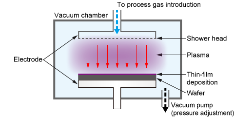
The main advantage of PECVD over conventional thermal CVD methods (often used in an epitaxial growth system) is its ability to form films at lower temperatures. This low-temperature process allows for deposition on substrates with complex topographies or those that cannot withstand high heat.
(2) Plasma dry etching
Etching is the process of creating grooves and patterns on a substrate surface. While wet etching uses chemical solutions, dry etching utilizing gas or ions has become the mainstream method in modern manufacturing.
Plasma dry etching, also known as chemical-physical etching, removes material from the substrate surface using plasma. Similar to PECVD, a process gas is ionized into plasma. The ions accelerate and collide with the substrate while reacting chemically with the surface material. This allows for precise, anisotropic removal of material at the atomic scale. This atomic-level precision is critical for defining the intricate patterns of electronic circuits, allowing more transistors to be packed into a smaller area. Common techniques include Reactive Ion Etching (RIE) using vacuum discharge plasmas such as Inductively Coupled Plasma (ICP) and Capacitively Coupled Plasma (CCP).
Unlike wet etching, this process does not generate liquid waste, making it a cleaner and more precise manufacturing method.
Deeper etching can also be used to separate semiconductor chips, known as plasma dicing. For dicing, please refer to "Back-End Semiconductor Manufacturing Process".
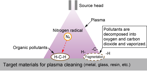
(3) Plasma cleaning
Plasma cleaning removes organic contaminants, such as oils, from substrate surfaces by decomposing and vaporizing them with plasma. This dry process eliminates the need for water or solvents, leaving no residue and ensuring a high level of cleanliness.
Additionally, plasma treatment can modify surface properties, such as increasing hydrophilicity by breaking molecular bonds and introducing hydroxyl groups. In semiconductor manufacturing, this technique is often used to improve adhesion on patterned surfaces like PDMS (polydimethylsiloxane).
Is fire a plasma?
A burning flame from a candle or firewood is often cited as an example of plasma. However, the brightness of a flame is primarily due to chemical reactions and heat, rather than pure ionization.
When fuel burns, carbon combines with oxygen, releasing energy as blue light (chemiluminescence). The bright yellow part of a flame typically results from incandescence (blackbody radiation) of soot particles heated to over 1,000°C.
Nevertheless, flames do exhibit plasma-like characteristics. They contain ionized particles and can conduct electricity more easily than the surrounding air. Shadows formed by flames in strong light also suggest the presence of ions scattering light.
While scientifically debated due to its relatively low ionization density compared to industrial plasmas, a flame can be considered a partial plasma. It serves as a complex example of matter bridging the gap between gas and plasma states.
Reference
- Samco Inc.
(https://www.samcointl.com/)
Recommended products
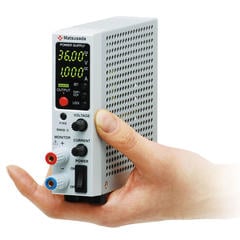
Matsusada Precision's products meet the stringent specifications required by the semiconductor industry, providing the stability and precision necessary for advanced plasma processes in the production of high-end electronic devices.