FPD refers to a Flat Panel Display device.
A Flat Panel Display (FPD) is a thin video display device that replaces the cathode-ray tube (CRT).
In the past, cathode ray tubes were mainly used as a device to display images. A cathode-ray tube is a device that emits an electron beam into a funnel-shaped vacuum tube and deflects it with a magnetic field to scan over the phosphor. The phosphor that the electron beam hits emits light and displays an image.
However, the disadvantage of cathode-ray tubes was that they required a lot of depth for the display because vacuum tubes were essential. FPDs, which have been increasing in number in recent years, do not require vacuum tubes and are therefore thinner than CRTs.
There are several types of FPDs, including liquid crystal displays (LCDs), plasma displays, organic electroluminescent displays, and LED displays, which are used in all kinds of electronic devices such as electronic paper and digital signage, as well as televisions and smartphones.
Mechanism of FPD
As mentioned above, there are various types of FPDs. Still, this section will explain the mechanisms of liquid crystal displays (LCDs) and organic EL displays, which are often used in electronic products.
How does a liquid crystal display (LCD) work?
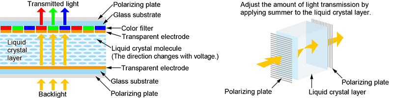
An LCD structure typically consists of a backlight followed by a rear polarizer, a glass substrate (TFT array), a liquid crystal layer, a color filter, a front glass substrate, and a front polarizer. The backlight remains constantly illuminated, and the image is created by controlling the amount of light that passes through the liquid crystal layer and color filters.
The liquid crystal layer acts as a light shutter. This mechanism relies on the interaction between the liquid crystals and the two polarizers. In a twisted nematic (TN) configuration, liquid crystal molecules naturally align in a twisted structure between two substrates with alignment films. This twist rotates the polarization of light, allowing it to pass through the front polarizer.
When voltage is applied to the liquid crystal layer, the molecules reorient themselves perpendicular to the substrates. This destroys the twisted structure, preventing the light's polarization from rotating. As a result, the light is blocked by the front polarizer. By varying the voltage, the amount of light transmission is precisely controlled, creating the grayscale levels required for image display.
The light emitted from the backlight passes through the polarizer, and only light with a wavelength in a certain direction reaches the liquid crystal layer. The grooves of the alignment film are oriented orthogonally to the grooves of the polarizer, so when no voltage is applied, the light from the backlight is blocked and does not appear on the surface.
However, the portion of the liquid crystal layer where voltage is applied allows light to pass through, so light passing through the color filter is recognized as an image. Thus, in a liquid crystal display (LCD), electricity is applied to the liquid crystal layer to let light through or block it, and to adjust the amount of light that passes through.
Mechanism of Organic Electroluminescent (OLED) Displays
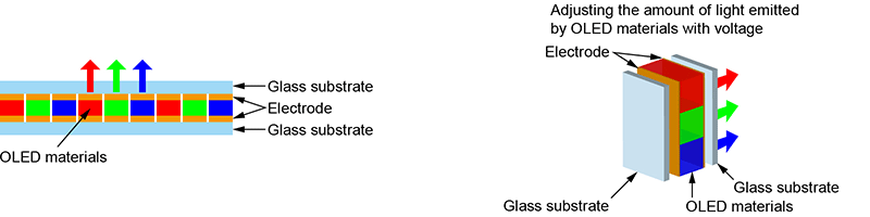
Unlike LCDs, OLED displays do not require a backlight. As a result, thinner and lighter FPDs can be realized, and their use in smartphones, game consoles, and TVs has been expanding in recent years.
The term "organic electroluminescence" is mainly used in Japan, while in Europe and the United States (in English), it is called OLED (Organic Light Emitting Diode).
An OLED display consists of three primary colors of OLED materials sandwiched between electrodes, and when voltage is applied, the OLED materials emit light directly.
Manufacturing process of FPD
So, what is the process of manufacturing FPDs?
The manufacturing process of liquid crystal displays (LCDs)
LCD manufacturing is broadly divided into array process, color filter, and module process. In the array process, in addition to circuit design and photomask manufacturing, TFT (Thin Film Transistor) manufacturing is carried out.
1. Array process
Circuit design: Design the arrangement of pixels, the smallest unit of display, and the circuits around the display.
Photomask fabrication: Making photomasks to be used for baking TFTs and color filters onto glass substrates.
Substrate cleaning: Using substrate cleaning equipment, remove dust on the glass substrate used as the base. The processes of film formation, lithography, and etching that take place in TFT manufacturing are similar to the front-end processes of semiconductor manufacturing.
Film formation: This step creates the transparent electrode film, gate electrode film, wiring film, and insulating films necessary for TFTs. Sputtering is commonly used for metal layers; in this process, argon ions strike a target material, ejecting atoms that deposit onto the glass substrate. For insulating layers, Plasma Enhanced Chemical Vapor Deposition (PECVD) is used, where source gases are converted into plasma to form thin films.
Resist coating: photoresist (photosensitive material) is coated on the thin film formed on the glass substrate.
Exposure: UV light is irradiated through a photomask onto the resist coated on the substrate to sensitize the areas not covered by the photomask.
Development: After exposure, the circuit pattern is developed by immersing the substrate in a developer. The developed photoresist serves to protect the underlying thin film in the subsequent process.
Etching: Etching of glass substrates using chemicals and ions. Etching removes the photoresist and thin film on the glass substrate, but the developed photoresist is not removed by etching and protects the thin film underneath. This gives the thin film the shape of a circuit pattern.
Resist stripping: removes the photoresist that has been developed and not removed by etching.
2. Color filter and module process
Color filter formation: Red, green, and blue color filters are formed by repeating the processes of film formation, resist coating, exposure, and development. After that, transparent resin, which serves as a protective film, is applied and cured.
Liquid crystal layer filling: The transparent electrodes that control the liquid crystal are formed by film deposition, resist coating, exposure, and development in the same way as the transparent electrodes of TFTs. After that, the resin is applied, and rubbing is performed to form grooves in the alignment film that align the orientation of the liquid crystal molecules. Fill the liquid crystal material and paste the TFT substrate and color filter together.
A polarizing plate, backlight pasting: Polarizing plate, driver IC terminal, backlight, etc., are pasted.
OLED display manufacturing process
The manufacturing process for OLED displays is divided into three parts: front-end process, deposition process, and back-end process.
1. Front-end process
In the front-end process, TFT circuits are made. This process is the same as the manufacturing process for liquid crystal displays.
2. Deposition process
In the vapor deposition process, three colors of organic materials, which are also light emitters, are deposited. In most cases, the deposition of organic materials is done by vapor deposition. The organic materials that emit red light are deposited first, followed by blue and green organic materials.
The deposition of organic materials is performed alongside the deposition of the hole injection and hole transport layers. Since organic emitting materials are not sufficiently conductive on their own, these auxiliary layers are essential for efficient voltage application.
Materials such as Copper Phthalocyanine (CuPc) or specialized amine derivatives are often used for the hole injection and transport layers. During vacuum evaporation, metal masks are used to pattern the organic layers, ensuring materials are deposited only in the required areas.
3. Back-end process
The back-end process involves encapsulation of the organic material, cutting of the panel, and connection of the wiring.
Reference (Japanese site)
- Semiconductor Equipment Association of Japan (SEAJ) - FPDとは
(https://www.seaj.or.jp/semi/about_fpd.html) - Semiconductor Equipment Association of Japan (SEAJ) - FPD製造工程とは
(https://www.seaj.or.jp/semi/lcd_proc/) - Semiconductor Equipment Association of Japan (SEAJ) - FPD製造工程 アレイ工程
(https://www.seaj.or.jp/semi/lcd_proc/array_process.html) - SCREEN - FPD製造プロセス フレキシブル有機ELディスプレー
(https://www.screen.co.jp/ft/products/process) - artience株式会社 - FPDとは
(https://www.artiencegroup.com/ja/products/colorfilter/fpd/about_fpd.html) - CANONトッキ - 有機ELの製造プロセス
(https://tokki.canon/organic_el/process.html) - 高分子論文集, Vol. 68, No. 1 (2011) - 有機EL素子の正孔注入層としてのポリアニリンナノ薄膜
(https://www.jstage.jst.go.jp/article/koron/68/1/68_1_45/_pdf)
Related Technical Articles
Related Products
Matsusada Precision manufactures and sells a variety of power supplies used in FPD and semiconductor manufacturing equipment.