


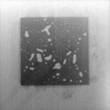
X-ray inspection plays a critical role in the quality control and failure analysis of power semiconductors and power modules. Reliable bonding between semiconductor dies--such as Silicon Carbide (SiC) or Gallium Nitride (GaN)--and substrates is achieved through advanced die-attach methods, including sintering and soldering.
During the bonding process, internal defects like voids, cracks, or shrinkage cavities can compromise heat dissipation, significantly affecting product performance and reliability. High-resolution X-ray inspection systems allow for the non-destructive detection of these hidden defects. This is particularly essential for modern power modules utilizing Direct Bonded Copper (DBC), Direct Brazed Aluminum (DBA), or Active Metal Brazing (AMB) substrates, where structural integrity is paramount.
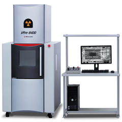
Recommended products
Related Technical Articles
- Back-End Semiconductor Manufacturing Process
- Selecting an X-ray Inspection System
- Principles of Radiography
- Safe Operation of X-ray Inspection Systems
- What is Microfocus X-ray Technology? (Basic Knowledge)
- Basics and Principles of Computed Tomography (CT)
- Non-Destructive Testing: Types and Applications
- What are X-rays? (Basic Knowledge)
- How to Acquire High-Quality Computed Tomography (CT) Images - X-ray NDT series (1)
- A Guide to X-ray CT Images: Formats, Viewing, and Applications - X-ray NDT series (2)
- X-ray Image Processing and Automated Inspection - X-ray NDT series (3)
- Types of X-ray Tubes and High-voltage Power Supplies
- What is the difference between Radioactivity, Radiation, and Radioactive Materials?
- Understanding Radiation: Effects on the Body and X-ray Safety