


Sputtering is a Physical Vapor Deposition (PVD) technique used to deposit thin films of material onto a substrate.
The process involves introducing an inert gas, typically argon, into a vacuum chamber containing a target material. When a high negative voltage is applied to the target, a glow discharge is initiated. Positive ions from the resulting plasma are accelerated toward the target, bombarding its surface at high speeds.
This bombardment ejects atoms from the target--a phenomenon known as sputtering. These ejected atoms travel through the vacuum and deposit onto the substrate, forming a precise thin film.
Sputtering is highly regarded for its ability to produce films with excellent thickness uniformity and density. It allows for precise control over film quality and is suitable for high-melting-point metals and alloys. Additionally, by introducing reactive gases, it creates high-quality oxide and nitride coatings.
Common applications include semiconductor wiring, barrier films, and transparent conductive films for smartphones and tablets. Sputtering is also widely used to create reflective coatings for automotive headlights and various decorative finishes.

- Related Terms:
-
- Physical Vapor Deposition (PVD)
- Plasma
- Semiconductor
- Flat Panel Display (FPD)
- Thin film
- Sputter
- High voltage
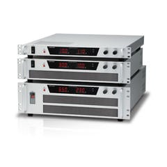
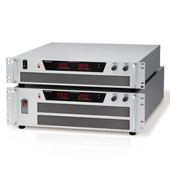
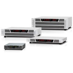
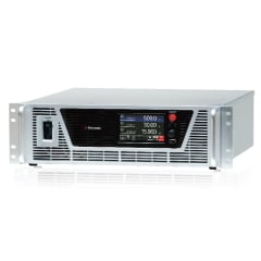
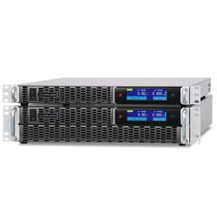
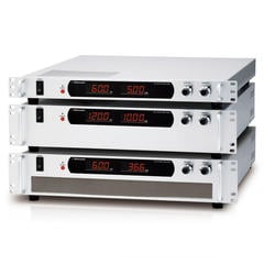
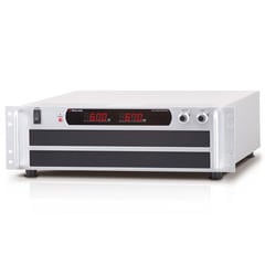
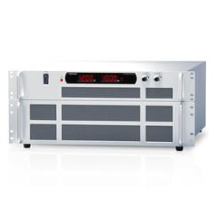
Recommended products
Power Supply Selection for Sputtering: Sputtering deposition typically uses DC power supplies for metal targets and RF (Radio Frequency) power supplies for insulating (dielectric) targets. RF is required for insulators to prevent "charge-up" on the target surface, which would otherwise extinguish the plasma discharge.
Important Note on Sputtering Applications: Sputtering processes often involve plasma instability and frequent arcing (abnormal discharge). Standard DC power supplies may require specific configurations or external protection to operate reliably under these conditions. To ensure the best performance and longevity of your system, please contact our sales department regarding your specific requirements before selecting a model. We can assist in configuring the optimal power solution for your vacuum deposition equipment.
Matsusada Precision offers a wide range of power supply solutions for vacuum and deposition processes. We also manufacture essential components such as electrostatic chuck power supplies and piezo drivers for semiconductor and FPD manufacturing equipment.
Related Technical Articles
- Front-End Semiconductor Manufacturing Process
- Back-End Semiconductor Manufacturing Process
- What is a Flat-Panel Display (FPD)? A Guide to Mechanisms and Manufacturing
- Plasma in semiconductor manufacturing
- Types of Power Semiconductors -Reliability and Performance Tests
- What is a power inverter?
- Safety and Usage of High Voltage Power Supply