Ion implantation, which modifies semiconductor characteristics, is a critical process in semiconductor manufacturing. This article provides an overview of the fundamental principles of ion implantation processes and equipment, along with an introduction to Matsusada Precision's products used in these applications.
Fundamentals of Ion Implantation
Let's begin by exploring the basic concepts of ion implantation, including its underlying principles and key parameters.
What Is Ion Implantation?
Ion implantation is a technique for introducing dopant atoms (impurities) into silicon and other semiconductor wafers. For wafers to function as electronic devices, specific impurities must be precisely introduced to create distinct p-type and n-type semiconductor regions. Consequently, ion doping is an indispensable step in semiconductor manufacturing.
While various ion doping methods have been developed, ion implantation offers the distinct advantage of enabling precise doping with extremely pure dopant species. This makes it the predominant choice for fabricating advanced semiconductor structures with fine geometries.
Operating Principles
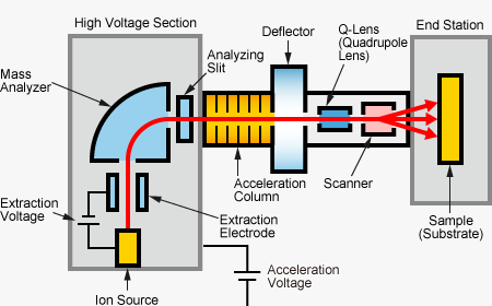
Next, let's examine the fundamental operating principles of ion implantation equipment. Ion implantation systems generate ions from an ion source, accelerate them to high energies, and precisely direct them using deflectors and scanning systems. This enables ions to be implanted at specific locations on the sample, thereby achieving controlled doping.
The process begins at the ion source, which contains the source material from which ions are generated. An electromagnetic field is applied to create plasma, which ionizes the source material by stripping away electrons to produce the desired ions.
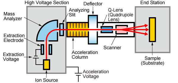
These ions then enter a mass analyzer, where they are separated based on their mass-to-charge ratio to isolate the specific ion species required. Only the target ions pass through the analyzing slit and proceed to the acceleration column, effectively preventing contamination from unwanted impurity ions. Within the acceleration column, a high-voltage electric field accelerates the ions to the energy levels necessary for successful implantation.
The accelerated ion beam then passes through beam-shaping and focusing elements, including deflectors and quadrupole (Q) lenses, which precisely control the beam's angle and focus. A scanning system sweeps the focused ion beam across the entire wafer surface to ensure uniform coverage. Ion implantation occurs when this controlled ion beam strikes the sample positioned in the end station.
Key Parameters
When performing ion implantation, proper configuration of equipment parameters is essential to achieve the desired results. The primary parameters are outlined in the table below:
| Parameter | Description |
|---|---|
| Dose | The number of ions implanted per unit area. Higher dose values result in greater ion concentrations. |
| Acceleration Energy | The kinetic energy imparted to ions for implantation into the substrate. Higher acceleration energies enable deeper ion penetration into the wafer. |
| Beam Current | A parameter that quantifies the ion charge as a measurable current value, used for dose calculation and monitoring. Higher beam currents enable faster doping processes but can cause substrate overheating. |
| Implantation Angle | The angle between the wafer surface and the incident ion beam. To prevent channeling effects (*), the angle must differ from the wafer's crystal orientation, typically tilted approximately 7 degrees from normal incidence. |
Note: Channeling is a phenomenon where ions penetrate abnormally deep along crystal lattice planes, compromising precise depth control during implantation.
Classification of Ion Implantation Systems
Ion implantation systems are classified into three categories based on their acceleration energy and beam current capabilities. The characteristics and applications of each type are described below.
Medium-Current Ion Implantation Systems
These systems operate at acceleration energies of 260 keV or below, with beam currents in the microampere range, making them suitable for low-dose implantation applications. They offer high energy efficiency and cost-effectiveness due to their relatively low energy and current requirements. Additionally, they provide wide-area, high-precision beam control, making them ideal for gate region processing and the formation of fine semiconductor structures.
High-Current Ion Implantation Systems
These systems are designed to deliver high beam currents in the milliampere range. Although their acceleration energy is limited to around 80 keV, this allows for the generation of significantly higher beam currents. This capability makes them especially well-suited for applications requiring high-concentration impurity doping in shallow regions, such as source and drain formation.
High-Energy Ion Implantation Systems
These systems deliver acceleration energies ranging from 250 keV to 7 MeV. Although they require large accelerator structures and involve higher costs, they can implant ions deep into wafer substrates, at depths not achievable with other systems. As such, they are essential for applications requiring deep implantation, including well structures, power devices, CMOS technologies, and X-ray sensors.
Process-Specific Ion Implantation
Next, we examine the various types of ion implantation used in semiconductor manufacturing processes, with a focus on MOSFET and other device fabrication.
Process Overview
Ion implantation in semiconductor manufacturing can be broadly categorized into three main process steps, as outlined in the table below:
| Process Step | Description |
|---|---|
|
Gate-Channel Formation (Medium Current) |
The process of forming the channel region beneath the gate electrode in MOSFETs and CMOS devices. Medium-current ion implantation systems are employed for precise, low-dose doping. |
|
Source-Drain High-Dose Implantation (High Current) |
The process of forming highly doped source and drain regions in field-effect transistors. High-current ion implantation systems are utilized to achieve the heavy doping concentrations required for low electrical resistance. |
|
Well and Deep Junction Implantation (High Energy) |
The process of creating n-well and p-well structures in transistors, as well as performing backside processing for power devices. High-energy ion implantation systems are used to achieve the deep penetration depths required for these applications. |
Gate-Channel Formation (Medium Current)
Medium-current ion implantation systems are employed for gate-channel region formation. The channel region is the area between the MOSFET's source and drain, where a depletion layer forms when charge accumulates at the gate electrode.
To ensure rapid depletion layer formation upon gate charging, the doping concentration must remain low, necessitating low-dose ion implantation. Precise implantation control is also essential to achieve uniform depletion layer expansion, making medium-current ion implantation systems the preferred choice for this application.
Source-Drain High-Dose Implantation (High Current)
High-current ion implantation systems are utilized for MOSFET source-drain region formation. As these regions must carry substantial currents, minimizing electrical resistance is critical. High-current systems enable heavy doping to achieve high impurity concentrations, thereby increasing conductivity and providing the low-resistance characteristics required for efficient device operation.
Well and Deep Junction Implantation (High Energy)
High-energy ion implantation systems are essential for creating well structures that serve as MOSFET foundations and for backside processing in power devices. For example, when fabricating an nMOSFET on an n-type substrate, p-type doping must be applied to the underlying foundation region. This region is formed as a deep, well-like structure-hence the term "well."
In power devices designed for vertical current conduction, backside electrode formation is required. This involves flipping the wafer and implanting ions to specific depths. Such deep implantation requirements make high-energy ion implantation systems indispensable for these applications.
Ion Implantation Process
Building on the overview provided in the "Principles" section, we now examine the ion implantation process in detail through eight distinct steps.
Process Overview
The complete ion implantation process is summarized in the table below:
| Step | Purpose |
|---|---|
| 1. Ion Generation | Generate ions from source materials for wafer implantation |
| 2. Ion Extraction | Separate generated ions from electrons and form an ion beam |
| 3. Mass Analysis | Use a mass analyzer to filter out unwanted ion species and select target ions |
| 4. Beam Acceleration | Provide ions with sufficient kinetic energy for successful wafer penetration |
| 5. Beam Transport/Focusing | Position and focus the ion beam for precise scanning control |
| 6. Beam Scanning | Direct the ion beam to specific locations across the wafer surface |
| 7. Implantation | Embed ions into the wafer substrate to achieve doping |
| 8. Annealing | Restore the crystal structure and electrically activate the implanted dopants through thermal treatment |
1. Ion Generation (Ion Source)
Ion generation refers to the creation of ions for wafer implantation by subjecting source materials in a vacuum chamber to intense electromagnetic fields, thereby producing a plasma. When matter is exposed to such fields, electrons are stripped from atomic nuclei, forming positive ions and free electrons-a phenomenon known as ionization. The resulting plasma, in which ions and electrons move freely, serves as an ideal medium for ion implantation.
2. Ion Extraction
Ion extraction involves selectively drawing ions from the plasma generated in the ion source to form an ion beam. This is achieved by applying high voltage to extraction electrodes, which create an electric field that accelerates the ions in a controlled direction. The process effectively separates ions from electrons and directs them to the next processing stage.
3. Mass Analysis
Mass analysis eliminates unwanted ion species that may be introduced by source material impurities or other contamination. This step leverages the mass differences between ion species to selectively separate the target ions.
Several methods are available for mass analysis, including magnetic sector analyzers, Q mass filters, and ion trap systems, each based on different separation principles. The appropriate method is selected based on the required resolution and selectivity. Following mass analysis, the ion beam is refined further using analyzing slits to enhance separation precision, ensuring that only the desired species proceed to the next stage.
4. Beam Acceleration
To achieve effective ion implantation, ions must be accelerated to high energies using acceleration voltages of tens of kilovolts or higher. The energy imparted during the initial ion extraction stage is insufficient to give ions the kinetic energy required to penetrate the wafer's atomic structure and ensure proper implantation. Therefore, additional high-voltage acceleration is applied to provide the ions with adequate energy for successful implantation into the target substrate.
5. Beam Transport and Focusing
This stage involves transporting and focusing the ion beam to ensure precise delivery to the intended target locations during scanning. The ion beam first passes through deflection systems that adjust its trajectory and position. It then enters Q lenses-electromagnetic focusing elements composed of four-pole magnetic or electrostatic fields-which converge the ion beam by applying focusing forces from four directions, creating a well-defined, focused beam profile.
6. Beam Scanning and Wafer Scans
In ion implantation systems, to ensure uniform doping across the entire wafer, either the ion beam or the wafer (or both) must be moved. Scanning methods are generally categorized into three types: electrostatic, mechanical, and hybrid scanning.
6.1 Beam Scanning Method (Electrostatic Deflection)
In many systems, the ion beam is scanned using electrostatic deflection. A triangular waveform generated by a high-voltage amplifier is applied to deflection electrodes, enabling the beam to sweep rapidly across the wafer. This method is common in medium-current implanters where high-speed scanning is required.
6.2 Ribbon Beam Method
The ribbon beam method utilizes an ion beam that has been shaped into a wide, elongated profile, often exceeding the diameter of the wafer. Unlike a scanned spot beam, a ribbon beam provides a constant line of ions. When combined with simple linear wafer translation (mechanical scanning in one direction), it ensures highly uniform implantation coverage without the need for high-frequency beam sweeping.
6.3 Mechanical Scan Method
The mechanical scan method achieves uniform implantation by moving the wafer itself through a stationary ion beam. This can involve a "two-dimensional" mechanical scan (moving the wafer in X and Y directions) or a "one-dimensional" scan (used with a ribbon beam or a scanned fan beam). This method is particularly effective for high-current implantation as it allows for better heat dissipation and maintains a constant incident angle across the entire wafer surface.
7. Implantation
Impurity doping is achieved when the scanned ion beam penetrates the wafer surface and becomes embedded within the substrate material. The end station housing the wafer is equipped with high-temperature heating fixtures positioned beneath the wafer's backside. These fixtures maintain the wafer at elevated temperatures during implantation to minimize crystal lattice damage caused by ion bombardment.
8. Annealing
Ion implantation damages the wafer's crystal structure, making a subsequent heat treatment process-called annealing-necessary to restore crystallinity and electrically activate the implanted dopants. Annealing is typically performed using rapid thermal processing with infrared radiation or laser heating to quickly reach the required temperatures. This approach minimizes thermal damage and helps prevent unwanted dopant diffusion that could compromise device performance.
Applications of Ion Implantation
Beyond the formation of standard MOSFETs and CMOS devices, ion implantation is a critical technology in the fabrication of a wide range of advanced semiconductors and power devices. Key applications include:
Superjunction MOSFETs (SJ-MOSFETs)
Superjunction MOSFETs achieve both low on-resistance and high breakdown voltage through a structure of alternating vertical n-type and p-type columns. High-energy ion implantation is essential for forming the deep p-columns, enabling precise doping at depths of several tens of micrometers. This meticulous control over the charge balance is crucial for achieving superior performance and is a key enabling technology for the mass production of 600 V to 1200 V class high voltage superjunction power devices.
SiC Power Devices
Silicon carbide (SiC) is a leading material for next-generation power devices, prized for its excellent high-voltage and high-temperature characteristics. Because thermal diffusion is notoriously difficult in the SiC crystal lattice, ion implantation is the indispensable method for doping. It is critically used to form the channel regions under the gate oxide, the p+ regions in Junction Barrier Schottky (JBS) diodes, and to define the precise channel structure of SiC JFETs.
IGBTs (Insulated Gate Bipolar Transistors)
IGBTs merge the voltage-controlled gate of a MOSFET with the high current-handling capability of a bipolar transistor. In IGBT fabrication, ion implantation is leveraged not only for creating p-wells and channel regions but also for forming the crucial field-stop (FS) layer on the collector side. This FS layer is vital for achieving higher breakdown voltages while simultaneously reducing switching losses.
CMOS Image Sensors
For CMOS image sensors, where high image quality and low noise are paramount, precise ion implantation is essential. This technology is used to define the photoelectric conversion regions (photodiodes) and to optimize charge transfer efficiency. It also plays a key role in precisely engineering the electric fields within deep photodiode structures and at pixel boundaries to minimize noise and crosstalk.
X-ray Sensors and Detectors
In the manufacturing of X-ray sensors and other high-sensitivity radiation detectors, high-energy ion implantation is used to create deep p-n junctions and other structures that ensure high charge collection efficiency. This capability is fundamental to developing the high-performance sensors required for advanced medical imaging and non-destructive testing (NDT) systems.
Ion Implantation Equipment Manufacturers
Next, we examine the leading ion implantation equipment manufacturers in the industry.
Applied Materials, Inc. (AMAT)
AMAT is the world's largest semiconductor equipment manufacturer, offering products that support a broad spectrum of semiconductor processing technologies. While the company maintains dominant market positions in deposition and etching equipment, it also provides diverse ion implantation systems that are widely adopted across the industry.
AMAT particularly excels in advanced node technologies, delivering precise beam control and ultra-low damage capabilities that have earned recognition for compatibility with 2 nm and 3 nm process nodes. The company's comprehensive product portfolio enables integrated solution delivery across multiple process steps.
Axcelis Technologies, Inc.
Axcelis Technologies is a leading American specialized manufacturer that has dedicated over 45 years to developing ion implantation solutions for the semiconductor industry. As a company focused primarily on ion implantation equipment, it stands as one of the most prominent global suppliers in this specific process step.
The company's flagship Purion™ platform provides complete product coverage, encompassing medium-current, high-current, and high-energy ion implantation systems. Axcelis is particularly renowned for its leadership in the high-energy segment and has built a strong market presence in applications for power devices (such as SiC and GaN) and advanced image sensors through its specialized platforms. Its systems are well-regarded for delivering exceptional beam purity, precise dose control, and a low total cost of ownership, making them widely adopted across memory, advanced logic, and mature process nodes.
Sumitomo Heavy Industries, Ltd.
Sumitomo Heavy Industries is a diversified manufacturer producing an extensive range of products, from mechanical components such as gear motors and inverters to industrial machinery including hydraulic excavators, presses, and injection molding equipment. The company has strategically focused on the semiconductor sector as a key growth area and offers a comprehensive portfolio of ion implantation systems.
Sumitomo develops medium-current, high-current, and high-energy ion implantation systems, providing complete product coverage across all application segments. Its global business presence enables comprehensive worldwide support capabilities.
Nissin Ion Equipment Co., Ltd.
Nissin Ion Equipment is a specialized manufacturer dedicated to ion implantation systems for the semiconductor and display industries. The company has earned strong market recognition for its advanced technological capabilities, achieving a remarkable 100% global market share in ion implantation equipment for high-resolution display manufacturing used in smartphones and tablets. Recently, it has expanded its focus to include semiconductor applications, demonstrating exceptional product development, particularly for SiC power devices. Nissin is also well-regarded for its high level of customization, accommodating customers with specialized requirements.
ULVAC, Inc.
ULVAC is a comprehensive vacuum technology company with vacuum systems as its core competency. In recent years, it has intensified its research and development efforts in semiconductor manufacturing equipment, developing specialized ion implantation systems for targeted applications, including SiC power devices and photovoltaic cells. A distinctive feature of its systems is the capability to perform room-temperature implantation without wafer heating, making them particularly suitable for applications requiring precise, low-thermal-budget doping processes.
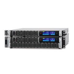
Matsusada Precision Power Supplies Supporting Ion Implantation Processes
Matsusada Precision offers a comprehensive lineup of power supply solutions specifically designed to support ion implantation processes.
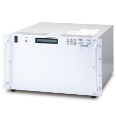
High-Voltage Power Supply for Acceleration
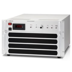
Ions must be accelerated by high voltages to penetrate the wafer effectively. High-energy ion implantation, in particular, requires exceptionally high voltage and power levels. Matsusada Precision's AUH series is engineered for this demanding application, delivering up to 200 kV and scalable to 52 kW in a master-slave configuration, providing the robust power necessary for deep implantation processes.
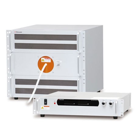
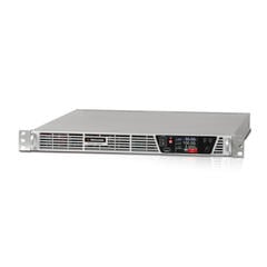
High-Voltage Power Supplies for Ion Source and Extraction/Suppression Applications
This high-voltage power supply series is engineered for ion generation, extraction, and secondary electron suppression applications. The systems offer excellent stability across voltage ranges from several kilovolts to tens of kilovolts. Multi-channel output configurations allow for application-specific power supply selection. Custom solutions-including power supplies beyond the standard lineup-are also available to accommodate diverse customer requirements.
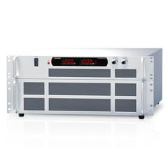
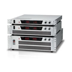
DC Power Supply (Constant Current) for Electromagnets
This series of constant current power supplies is designed for mass analysis magnets and beam control coils. During mass analysis, even slight fluctuations in the electromagnet's current can alter the ion beam's trajectory, allowing unwanted ions to pass through and contaminate the wafer. Featuring ultra-low ripple of 10 ppm and exceptional stability, these power supplies ensure consistent magnetic fields. This high precision enables accurate ion selection, contributing to higher device quality and improved manufacturing yields. Built-in protection circuitry ensures high reliability and system integrity.
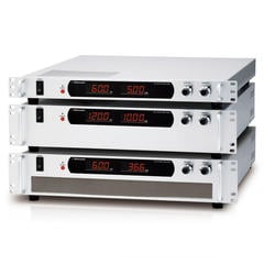
High Voltage Amplifier/High Voltage Pulse Power Supply
This high-speed pulse power supply series supports ion beam deflection and rapid scanning applications. The systems operate at frequencies up to 50 kHz and feature superior rise time performance along with precise, repeatable control. These characteristics contribute significantly to improved wafer uniformity and enhanced processing throughput.