A bipolar power supply operates across both positive (+) and negative (-) polarities, seamlessly crossing through zero. Unlike standard DC power supplies (unipolar) that only source current, bipolar supplies can both source and sink current.
This four-quadrant operation allows a single unit to function as a:
- DC Power Supply
- AC Power Source
- Electronic Load
- Amplifier
This versatility makes them essential for advanced R&D, component testing, and system integration.
High Voltage Amplifier (HV Amplifier)
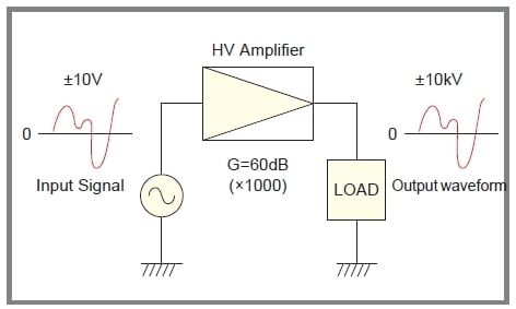
A high-voltage amplifier converts a low-voltage input signal into a high-voltage output waveform (Figure 1). Demand for these amplifiers is growing as they become indispensable tools for research, development, and system integration in fields such as electronics, physics, biochemistry, and medicine. Leveraging our advanced high-voltage technology, Matsusada Precision offers a diverse range of high-voltage amplifiers designed to meet a wide variety of customer requirements. * In addition to the models featured here, we also develop amplifiers specifically for applications such as electrostatic chucks (E-chucks) and PZT drivers. For more information, please contact our sales team.
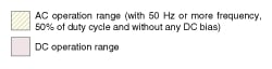
Four-Quadrant Output Range
Our high-voltage amplifiers feature a four-quadrant output, meaning they can both source (supply) and sink (absorb) current. This capability ensures stable voltage operation regardless of the load type (e.g., capacitive or inductive). Their fast response makes them ideal for applications requiring high-speed AC or arbitrary waveform outputs.
All Matsusada Precision high-voltage amplifiers (excluding some models) are bipolar, enabling true four-quadrant operation (Figure 2).
- Vomax: Rated output voltage
- Iomax: Rated output current
Slew Rate
The slew rate is the maximum rate of change of the output voltage and is a key indicator of an amplifier's response speed. It is expressed as dV/dt, typically in V/μs. For a given slew rate, a smaller output amplitude results in a shorter response time.
Our highest-performing AMPS series, for example, achieves a slew rate of over 1200 V/μs.
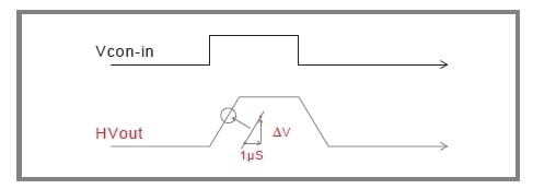
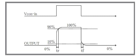
Rise Time (step response)
Step response can be indicated by the rise time, as shown in Figure 4. The rise time of an amplifier with a frequency response (= bandwidth) of fc (Hz) is typically given by the following formula.
tr ≅ 0.35/fc
The fall time (tf) is equal to tr.
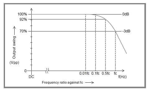
Frequency Response
Frequency response is specified as the frequency (fc) at which the output amplitude attenuates to approximately 70.7% (-3 dB) when driving a rated resistive load with a sinusoidal waveform.
Selection Guide: To ensure accurate waveform reproduction with minimal phase shift or distortion, select a model with sufficient bandwidth margin:
- Sinusoidal Waveforms: 3 to 5 times the operating frequency.
- Square Waveforms: At least 10 times the operating frequency (to preserve edge sharpness).
Insufficient bandwidth results in reduced amplitude and significant phase shift. Always verify the output waveform against your specific requirements.
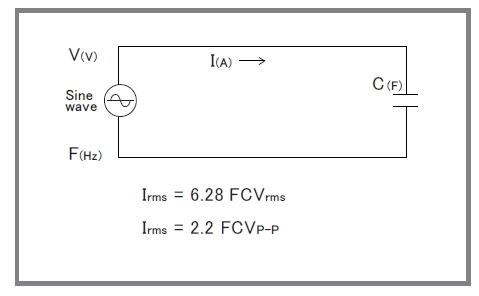
Driving Capacitive and Discharge Loads
Connecting capacitive loads exceeding 100 pF (including cable stray capacitance) may cause output oscillation. To stabilize the output, insert a high-voltage resistor in series with the load.
- Typical Values: 100 Ω (for 0.1 μF) to 1000 Ω (for 1000 pF)
Note: A series resistor forms a low-pass filter with the load capacitance, limiting the frequency bandwidth.
For applications involving electrical discharge (e.g., corona discharge), transient currents may exceed the amplifier's ratings. Always use a series protection resistor to limit current and prevent permanent damage.
Optimizing Performance: Cabling and Connections
We strongly recommend using non-shielded high-voltage cables for high-speed AC output. Shielded cables introduce significant stray capacitance (C) between the conductor and the shield. During high-speed voltage changes (dV/dt), this capacitance draws excessive charging current (i), leading to:
1. Reduced Slew Rate: The amplifier's current capacity is consumed by charging the cable rather than driving the load.
2. Waveform Distortion: Increased load on the amplifier.
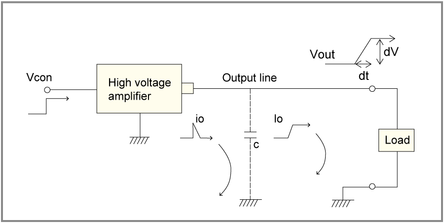
Charging current due to stray capacitance "C" from the output cable.
Solution
Minimizing Stray Capacitance To minimize the effects of stray capacitance from the output cable:
- Keep the cable as short as possible.
- Route the cable away from any conductive surfaces such as floors, desks, or metal chassis.
- Use non-shielded high-voltage cables.
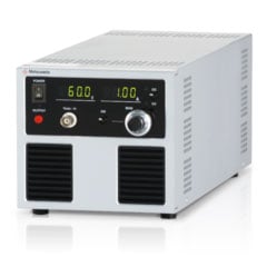
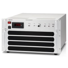
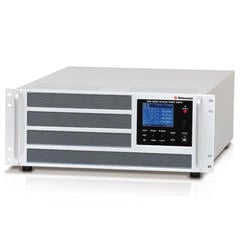
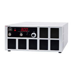
Recommended products
Matsusada Precision has a long track record and an extensive lineup to meet your bipolar power supply or high voltage amplifier requirements.