A diode is an electronic component that allows electric current to flow predominantly in one direction. Diodes are considered active components and are fundamental semiconductor devices. Their functions include rectifying current (regulating the flow of electricity), voltage regulation (maintaining a constant voltage), and signal demodulation (extracting signals from radio waves).

How Diodes Work
First, let's review the properties of semiconductors, the materials used to make diodes. Materials are classified as conductors, semiconductors, or insulators based on their ability to conduct electricity. A semiconductor, as its name suggests, is a material with electrical conductivity between that of a conductor (which readily conducts electricity) and an insulator (which does not).
Metals are good conductors of electricity because when metallic elements bond, their valence electrons become delocalized, forming a sea of 'free electrons.' When a voltage is applied, these free electrons can easily move through the metal's crystal lattice, carrying an electric charge and thus allowing current to flow.
A semiconductor is a material that can be made to act as a conductor or an insulator. Intrinsic (pure) semiconductors have far fewer free electrons than metals at room temperature. In semiconductors, current can be carried by two types of charge carriers: electrons (negatively charged) and holes (effectively positive charges representing the absence of an electron). When a voltage is applied, electrons can move, and holes can also appear to move as electrons fill them.
Semiconductors can be doped to become either p-type or n-type, differing in their primary charge carriers. In p-type semiconductors, the majority charge carriers are holes, and current flows as electrons move sequentially to fill these holes. P-type semiconductors are typically created by doping a tetravalent element like silicon with a trivalent impurity (an element with three valence electrons), such as boron or gallium. This doping creates an abundance of holes (positively charged carriers) compared to free electrons. The majority carriers, holes, behave as positive charges.
In n-type semiconductors, the majority charge carriers are electrons. N-type semiconductors are created by doping a tetravalent element like silicon with a pentavalent impurity (an element with five valence electrons), such as phosphorus. This introduces excess electrons into the material. The majority carriers are electrons, which are negatively charged.
When a p-type semiconductor is joined with an n-type semiconductor, a PN junction is formed. In a PN junction diode, the electrode connected to the p-type material is called the anode (A), and the electrode connected to the n-type material is called the cathode (K) (see Figure 1).

When a p-type and an n-type semiconductor are joined, electrons from the n-type material diffuse into the p-type material, and holes from the p-type material diffuse into the n-type material. This diffusion creates a region near the junction depleted of mobile charge carriers, known as the depletion region (or 'depletion layer'). Therefore, when a negative voltage is applied to the anode (p-type side) and a positive voltage to the cathode (n-type side) - a condition known as reverse bias - the electrons in the n-type material are attracted away from the junction towards the positive terminal, and holes in the p-type material are attracted away from the junction towards the negative terminal. This widens the depletion region ('depletion layer'). As a result, very little current flows through the diode (see Figure 2). This is the reverse-biased state.
Conversely, if a positive voltage is applied to the anode and a negative voltage to the cathode - a condition known as forward bias - holes in the p-type material are repelled towards the junction, and electrons in the n-type material are repelled towards the junction. If the applied voltage is sufficient to overcome the potential barrier of the depletion region, these charge carriers can cross the junction and recombine. This allows a significant current to flow from the anode to the cathode (conventional current flow, while electrons move from cathode to anode) (see Figure 3).
Thus, diodes exhibit the property of allowing significant current flow primarily in one direction (forward bias) while blocking current flow in the opposite direction (reverse bias). Light-Emitting Diodes (LEDs), common in everyday applications, are a special type of diode designed to emit light when current flows through the PN junction due to the recombination of electrons and holes. Diodes are extensively used in countless electronic applications that support our daily lives.
The Role of Diodes
Diodes have several primary functions, including:
(1) Rectification
Rectification is the process of converting alternating current (AC), which periodically reverses direction, into direct current (DC), which flows in only one direction. Diodes achieve this by allowing current to pass only during the positive (or negative, depending on orientation) half-cycle of the AC waveform, effectively blocking the other half-cycle or redirecting it (in full-wave rectifiers).
(2) Radiowave Detection
Signal Demodulation (Wave Detection): Diodes are used to extract information (e.g., an audio signal) from a modulated radio wave. This process, often called demodulation or detection, utilizes the diode's ability to rectify the high-frequency carrier wave, allowing the lower-frequency information signal to be recovered.
(3) Voltage Regulation
Voltage Regulation: While standard diodes are designed to block current in the reverse direction, Zener diodes are specifically designed to operate in the reverse breakdown region. When the reverse voltage across a Zener diode exceeds a specific value (the Zener voltage, VZ), it begins to conduct current while maintaining a relatively constant voltage across it, even if the current changes. This property is used for voltage regulation.
(4) Current conversion
Photodetection and Photovoltaic Effect: Some diodes, known as photodiodes, are designed to convert light energy into electrical current. When light strikes the PN junction, it can generate electron-hole pairs, leading to a current flow. This is the principle behind solar cells (photovoltaic cells), which act like a battery when illuminated and generate a voltage. Photodiodes are used in light detection applications, including infrared remote controls, responding to various wavelengths of light.
Types of Diodes
Various types of diodes exist, each designed for specific characteristics and applications. Some common types include:
Silicon diodes
Rectifier Diodes (often Silicon Diodes): These are the most common PN junction diodes, primarily used for rectification purposes in power supplies.
Germanium diodes
Germanium Diodes: These PN junction diodes have a lower forward voltage drop (around 0.3V) compared to silicon diodes (around 0.7V). This made them suitable for signal detection (demodulation) in early radio receivers, especially for weak signals. However, due to their higher leakage current, temperature sensitivity, and the advent of Schottky diodes, their use has declined.
Schottky diodes
Schottky Diodes: Formed by a metal-semiconductor junction (instead of a PN junction), Schottky diodes offer a very low forward voltage drop (typically 0.15V to 0.45V) and extremely fast switching speeds due to the absence of minority carrier storage. They are widely used in high-frequency applications, power supplies, and as rectifier diodes where low forward voltage drop and speed are critical.
Switching diodes
Signal Diodes (Switching Diodes): These are small-signal diodes designed for fast switching applications, effectively acting like an electronic switch. They turn ON (conduct) when forward biased and OFF (block current) when reverse biased. They are characterized by fast recovery times.
Fast recovery diodes (FRD)
A fast recovery diode (FRD) is a PN junction diode capable of high-speed operation. It is a type of high-speed diode with a shorter reverse recovery time (trr) compared to general rectifier diodes. This short trr minimizes switching losses, especially in high-frequency applications. FRD quickly reduces the reverse recovery current when switching from the forward conduction state to the reverse blocking state, allowing it to transition to the off state more efficiently and thereby reducing switching losses.
Therefore, it is commonly used as a rectifier diode in high-voltage switching power supplies and power factor correction (PFC) circuits for boost converters.
Esaki diodes
Tunnel Diodes (Esaki Diodes): Named after Nobel laureate Leo Esaki, these diodes utilize the quantum mechanical tunneling effect. They exhibit a region of negative differential resistance in their forward I-V characteristics, which allows them to be used in oscillators and amplifiers at very high frequencies (microwave range). They are made from heavily doped PN junctions.
Light-emitting diodes (LED)
Light-Emitting Diodes (LEDs): LEDs are PN junction diodes that emit light when forward biased. When electrons and holes recombine at the junction, energy is released in the form of photons (light). The color of the light depends on the semiconductor material used. While its primary function is illumination and indication, it inherently allows current to flow in one direction like other diodes.
Zener diodes
Zener Diodes: As mentioned earlier, Zener diodes are designed to operate reliably in the reverse breakdown region. They provide a stable reference voltage and are commonly used for voltage regulation and overvoltage protection.
New Generation SiC-SBD
SiC-SBD (Silicon Carbide Schottky Barrier Diode) utilizes silicon carbide, a wide-bandgap semiconductor material. Compared to conventional Silicon (Si) SBDs, SiC-SBDs offer significantly higher breakdown voltages and superior thermal conductivity. While their forward voltage drop (VF) varies by design, their primary advantage lies in switching performance. SiC-SBDs exhibit negligible reverse recovery time (trr) and dramatically reduced reverse recovery charge, resulting in minimal switching losses even at high frequencies and high voltages.
Due to these characteristics, SiC-SBDs are ideal for high-efficiency power conversion systems, including switching power supplies, solar inverters, and electric vehicle (EV) powertrains, where they help improve efficiency and reduce component size.
Below is a comparison between Si-SBDs, Si-FRDs and SiC-SBDs.
| Characteristic | Si-SBD | Si-FRD | SiC-SBD |
|---|---|---|---|
| Silicon Schottky Barrier Diodes | Silicon Fast Recovery Diodes | Silicon Carbide Schottky Barrier Diodes | |
| Material | Silicon (Si) | Silicon (Si) | Silicon Carbide (SiC) |
| Reverse Breakdown Voltage (VR or VBR) | ≤200 V | 200-1200 V | 650-1700 V |
| Forward Voltage Drop (VF) | 0.3-0.7 V | 1.2-2.0 V | 1.0-1.8 V |
| Reverse Leakage Current (IR) | Highest, increases significantly at high temperatures | Low, moderate increase at high temperatures | Low, minimal increase at high temperatures |
| Reverse Recovery Time (trr) | Very short (few ns) | Moderate (tens to hundreds of ns) | Extremely short (~few ns) |
| Switching Loss | Low | High | Very low |
| Operating Temperature | Up to ~150°C | Up to ~175°C | Up to ~200°C |
| Application Range | Low-voltage power supplies, RF applications | High-voltage rectifiers, power electronics | High-voltage, high-efficiency applications (EVs, industrial power, renewable energy) |
Comparison Results
Si-SBD: Ideal for low-voltage, high-speed applications, but has the disadvantages of high leakage current and low breakdown voltage. Also, their reverse leakage current (IR) increases significantly with temperature, which can be a limitation in thermally challenging environments.
Si-FRD: Suitable for applications below 1000V with medium switching speeds of 10- 50 kHz. They have a reverse recovery time (trr) typically ranging from tens to hundreds of nanoseconds. During this time, stored minority carriers in the PN junction must be removed, leading to transient reverse current and associated switching losses.
SiC-SBDs: SiC-SBDs offer high breakdown voltage, excellent thermal performance, and very low switching losses, making them ideal for high-power, high-efficiency applications.
While some FRDs are optimized for low forward voltage, their reverse recovery characteristics can still lead to significant switching losses compared to SiC-SBDs, especially as frequency and voltage increase.
For this reason, SiC-SBDs are advantageous in circuits involving high-frequency switching.
SiC-SBDs are devices that achieve high voltage resistance, low loss, and high-speed switching, contributing to higher power supply efficiency, higher-frequency operation, and more compact components. They are increasingly being used in Power Factor Correction (PFC) circuits and inverters for applications such as air conditioners, server power supplies, solar (photovoltaic) inverters, and electric vehicle (EV) fast chargers.
Further Evolution: SiC Super Junction SBD
SiC-SBD technology continues to advance, with the SiC Super Junction Schottky Barrier Diode (SiC-SJ-SBD) emerging as a key development.
Originally developed for high-voltage power MOSFETs, the super junction (SJ) structure overcomes the trade-off between on-resistance and breakdown voltage. Applying this architecture to SiC-SBDs can reduce specific on-resistance (RonA) by approximately 35-40% compared to conventional planar SiC-SBDs.
In 650 V class devices, this approach lowers the forward voltage (VF) by approximately 0.1-0.15 V at the same current density, directly reducing conduction losses. Furthermore, the improved figure of merit (FOM)--the product of on-resistance and junction capacitance--significantly lowers switching losses. These benefits become even more pronounced in high-voltage applications of 1.2 kV and above.
These improvements can boost power conversion efficiency by 0.5% to 1% or more in switching power supplies operating at high frequencies. Reduced heat generation simplifies cooling requirements and enables higher frequency operation, allowing for smaller passive components like inductors and capacitors. By contributing to higher power density and reduced total system costs, SiC-SJ-SBDs are expected to play a critical role in data center server power supplies and next-generation EV onboard chargers.
Related Technical Articles
Recommended products
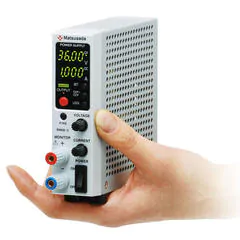
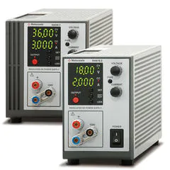
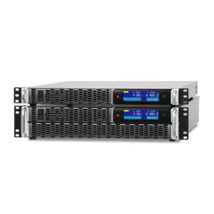
Matsusada Precision's high-voltage and DC power supplies are ideal for testing diodes and other semiconductors.