What is a scanning electron microscope?
A Scanning Electron Microscope (SEM) utilizes an electron beam to acquire magnified images of surface structures, achieving magnification levels ranging from tens to over one million times. Compared to visible light, electron beams have significantly shorter wavelengths, enabling the analysis of surface topography and material composition with far greater resolution than optical microscopes.
Structure of the electron gun
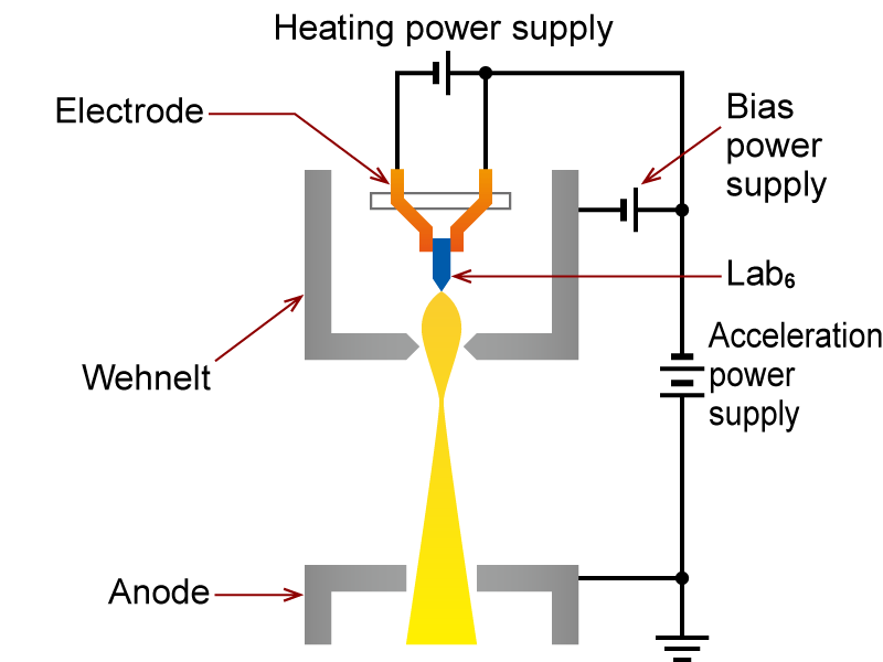
The electron gun is the equivalent of the light source in an optical microscope. Depending on the material of the filament and the method of electron generation, electron beams with different characteristics are generated.
| The tungsten-type thermionic emission gun | Lanthanum hexaboride (Lab6) thermionic emission gun |
|---|---|

|
|
|
Emitter material: Tungsten wire Luminance: 104 - 105 (A / cm2 / sr) Vacuum: 10-3 (Pa) Applications: benchtop SEM to general-purpose SEM |
Emitter material: LaB6 Luminance: 106 (A / cm2 / sr) Vacuum: 10-5 (Pa) Applications: General-purpose SEM |
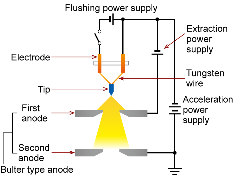
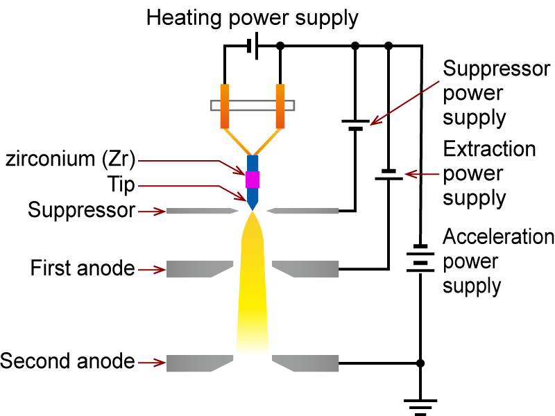
| Cold Field Emission Gun (Cold FEG) | Schottky Field Emission Gun (Schottky FEG) |
|---|---|
|
|
|
Emitter material: Tungsten single crystal Luminance: 109 (A / cm2 / sr) Vacuum: 10-8 (Pa) Applications: High-resolution SEM |
Emitter material: Zirconia/Tungsten Luminance: 108 (A / cm2 / sr) Vacuum: 10-7 (Pa) Applications: Analytical SEM |
Objective Lens Structure
The objective lens is the most important lens for focusing the image. There are three main types of objective lenses depending on the position of the sample and the shape of the pole piece.
| Out-lens | In-lens | Semi-in-lens |
|---|---|---|

|

|

|
| This is the most common objective lens configuration. The sample is placed below the objective lens for observation. Since the magnetic field leakage is lower than in other lens types, it allows for the observation of a wide variety of samples, including magnetic materials. | This objective lens achieves extremely low aberration by placing the sample directly within the magnetic field. Although observing large samples or magnetic materials is difficult, combining this design with a Field Emission Gun (FEG) yields the highest possible resolution. | This objective lens design serves as an intermediate solution between the out-lens and in-lens systems. By optimizing the pole piece geometry to utilize magnetic field leakage, it enables observation at a shorter working distance compared to the out-lens method. |
Effect of Accelerating Voltage on Image Appearance
The appearance of the image varies greatly depending on the acceleration voltage. This is because the electron scattering region of the primary electron beam differs depending on the acceleration voltage and the composition, density, and crystal orientation of the sample. The heavier the element and the lower the acceleration voltage, the smaller the electron scattering area and the more sensitive the SEM image. Using a lower acceleration voltage makes it possible to observe the fine texture of light elements, which is not visible at higher acceleration voltages.


The penetration depth of primary electron beam due to the difference in acceleration voltage
1 keV

5 keV

10 keV

Retarding Method (Deceleration Method)
The retarding method involves applying a negative voltage to the sample stage to decelerate the primary electron beam immediately before it reaches the sample surface. For example, if the primary electron beam is accelerated to 5.0 kV at the electron gun and -4.0 kV is applied to the sample, the beam is decelerated by the negative potential, resulting in a landing energy of 1.0 kV (5.0 kV - 4.0 kV). This method allows the primary beam to pass from the electron source to the objective lens at a high acceleration voltage, minimizing aberrations. This enables high-resolution observation even at low landing energies, which is superior to generating a 1.0 kV beam directly at the gun.


Sample: WS2 powder

Sample: WS2 powder
Major analysis using scanning electron microscopy
When a sample is irradiated with an electron beam, a lot of signal information is generated in addition to secondary electrons and reflected electrons. From there, various analyses can be performed, such as characteristic X-ray analysis (EDS and WDS), backscattered electron diffraction (EBSD), and electron beam induced current (EBIC). This article will discuss energy dispersive X-ray analysis (EDS), which is often used in SEM.
Energy Dispersive X-ray Spectroscopy (EDS)
When a sample is bombarded with an electron beam, characteristic X-rays are emitted. An Energy Dispersive X-ray Spectrometer (EDS) detects these X-rays to identify the elemental composition of the sample. Combined with SEM imaging, EDS enables elemental analysis and mapping at the micrometer scale.


Related Technical Articles
Related Products
Matsusada Precision manufactures precision high-voltage power supplies for scanning electron microscopes.