Acceleration Voltage of Electron Microscope
The electron microscope is an indispensable instrument for analyzing samples. This series explains the basics of electron microscopes. The first theme is the acceleration voltage of the electron microscope.
An electron microscope is a device that uses an electron beam to obtain an enlarged image of an observation object (hereinafter referred to as a sample). An electron beam consists of a stream of electrons focused and emitted in a specific direction. When viewed as a wave, the electron beam has a significantly shorter wavelength than visible light. This property allows for observation at much higher magnifications--or more precisely, higher resolutions--than is possible with optical microscopes.
In an electron microscope, electrons are accelerated by applying a high voltage emitted from the electron gun, converged by a focusing lens (converging coil) using an electromagnet, and then applied to the object to be observed. In the case of a transmission electron microscope (TEM), when the sample is made thin, the electron beam will be transmitted. If this transmitted electron beam is guided to the fluorescent screen via the objective lens, intermediate lens, and magnifying lens, the brightness of the fluorescent screen varies depending on the number of transmitted electrons. This can be imagined by shooting with a camera.
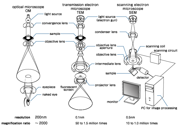
In the case of a scanning electron microscope (SEM), an electron beam is applied to the sample via a focusing coil, a scanning coil, and an objective lens. By narrowing down the electron beam as much as possible and scanning the surface, the secondary electron generated according to the shape of the sample hit by the electron beam is observed with a detector to obtain an image.
How can I increase the resolution of the electron microscope? Unlike the optical microscope, the following formula for the resolution is used for the electron microscope (TEM).
d = 0.65 (Csλ3) 1/4
d is the resolution, Cs is the spherical aberration coefficient, and λ is the wavelength of the electron beam. From this formula, to increase the resolution, in other words, to decrease the value of d, either decrease Cs or decrease λ. However, since it is difficult to improve Cs with an electron lens such as a focusing lens used in an electron microscope, the resolution is generally increased by reducing the wavelength λ.
The relationship between the wavelength λ of the electron beam and the acceleration voltage V is expressed by the following equation.
λ = 1.23/V1/2 (nm)
For example, if the electron acceleration voltage is 100 kV, the wavelength is 3.9 x 10⁻³ nm. If Cs = 0.5 mm, the resolution d is as follows.
- d = 0.65 {0.5 x 106 x (3.9 x 10-3)3}1/4
- = 0.65 {2.97 x 10⁻²}1/4
- = 0.27
Therefore, if the acceleration voltage is increased to 400 kV, the resolution is calculated to be less than 0.1 nm. Although the calculation formula is different in SEM, the resolution is basically improved by increasing the acceleration voltage.
However, increasing the acceleration voltage presents certain challenges. According to Einstein's special theory of relativity, the mass of an electron increases as its velocity approaches the speed of light. Consequently, as the acceleration voltage rises, the wavelength shortens less effectively than predicted by classical mechanics, limiting the expected improvement in resolution.
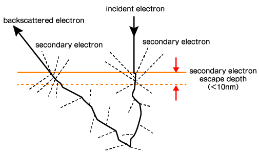
The resolution will also be affected. For example, in the case of SEM, secondary electrons due to reflected electrons are generated in addition to secondary electrons due to incident electrons. When the acceleration voltage is increased, the electrons are reflected after reaching a deeper position on the sample, and the reflected electrons come away from the incident position, making it impossible to examine the fine structure of the surface.
In addition, since the energy of electrons increases when the acceleration voltage is high, when the sample is an insulator, problems such as surface charging will occur. In order to avoid this in SEM, when using an insulating material as a sample, a pretreatment is required to apply a coating by depositing a conductor.
These challenges highlight two historical approaches to improving resolution. One approach focused on shortening the electron beam wavelength by increasing acceleration voltage. The other approach focused on reducing the spherical aberration coefficient (Cs) of the lenses. Advances in aberration correction technology now allow for improved resolution even at lower acceleration voltages.
In addition, SEM also employs a method in which the acceleration voltage is lowered to prevent the insulator surface from being charged.
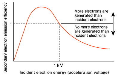
The efficiency of secondary electron emission decreases as the acceleration voltage exceeds 1 kV. A low secondary electron yield can cause sample charging. However, at an acceleration voltage where the yield is exactly 1 (known as the crossover point), no net charging occurs. Therefore, SEM eliminates the need for coating as a pretreatment if the acceleration voltage is used.
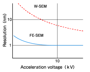
However, simply reducing the acceleration voltage is not enough. Lowering the acceleration voltage means increasing the wavelength of the electron beam, so the resolution will inevitably decrease. In particular, the resolution rapidly drops below a few kV. This is because aberration occurs due to variations in the energy of electrons emitted from the electron gun.
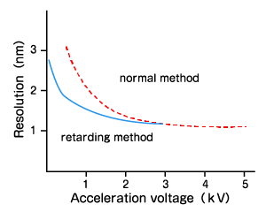
The "retarding method" offers a solution to this trade-off. In this method, electrons are emitted from the electron gun at a high acceleration voltage to minimize energy spread (chromatic aberration), and then a decelerating electric field is applied near the objective lens just before the beam strikes the sample. This technique allows the beam to land on the sample at a low landing energy while maintaining the high resolution associated with high-voltage transport.
In this case, since aberrations are reduced, there is an advantage that higher resolution can be maintained than when observing at normal low acceleration voltage. Of course, it will be necessary to add a circuit to the objective lens, so the structure itself will be a little complicated.
At this time, a method in which a circuit is added to the objective lens to decelerate the electrons while passing through the objective lens is called an "immersion lens method". On the other hand, a method in which the electron is decelerated before it collides with the sample after passing through the objective lens is called a "cathode lens method".
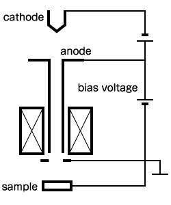
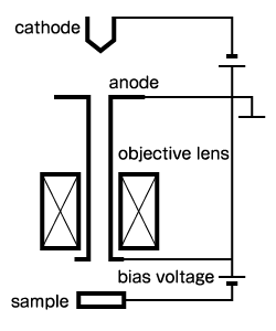
In the immersion lens method, the electric field near the sample is weakened, so the surface shape of the sample does not easily affect the lens characteristics. On the other hand, the cathode lens method has the advantage that higher resolution can be obtained by increasing the deceleration electric field.
Then, how should we set the optimum accelerating voltage according to the material of the sample based on these? In the case of TEM, the correct answer is to consider how fine you want to see the structure and apply an acceleration voltage to obtain the desired resolution.
In SEM, the optimal acceleration voltage depends heavily on the analytical purpose. For surface imaging, lower voltages are often preferred to visualize fine surface structures. However, for elemental analysis, the voltage must be sufficient to excite the characteristic X-rays of the target elements.
For example, to detect Iron (Fe), the acceleration voltage must be high enough to excite the Kα line (6.40 keV), typically requiring at least 7.11 kV. Conversely, lighter elements or lower energy lines like the Fe Lα line (0.70 keV) can be excited at much lower voltages. Therefore, operators must select an acceleration voltage that balances spatial resolution with the excitation energy required for the specific elements present in the sample.
In conclusion, the choice of acceleration voltage is a critical parameter in scanning electron microscopy that involves a trade-off. While high acceleration voltages are essential for achieving high-resolution imaging, they can cause sample damage and charging effects. Conversely, low voltages are ideal for observing surface details of insulating materials and for specific elemental analyses. Modern SEMs equipped with technologies like the retarding method allow operators to harness the benefits of low-voltage imaging without significantly sacrificing resolution. Ultimately, optimizing the acceleration voltage according to the sample material and the specific analytical goal is the key to obtaining high-quality and meaningful data.
Next time, as an electron microscope (SEM) technical explanation series (2), we will introduce the electron microscope lens.
Related Technical Articles
Recommended products
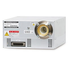
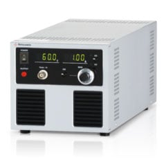
Matsusada Precision manufactures precision power supplies for scanning electron microscopes. That is multi-channel power supplies for electron guns, high-voltage modular power supplies for secondary detectors, and bipolar power supplies for magnetic lenses in SEM.
Reference (Japanese site)
- Japanese source page 「電子顕微鏡(SEM)技術解説シリーズ① 電子顕微鏡の加速電圧と画像の関係」
(https://www.matsusada.co.jp/column/sem1.html) - 電子顕微鏡の原理(一般社団法人 日本分析機器工業会)
(https://www.jaima.or.jp/jp/analytical/basic/em/principle/) - わかる入門講座:ナノテクの世界、その9(物質・材料研究機構)
https://www.nanonet.go.jp/pages/about_nanotech/primer/nano09.html - 球面収差補正による高分解能電子顕微鏡法の分解能向上(日本結晶学会誌 Vol.47, (2005) pp20-25)
(https://www.jstage.jst.go.jp/article/jcrsj1959/47/1/47_1_20/_pdf) - 表面分析研究会 電子光学入門(Journal of Surface Analysis Vol.14, No. 3 (2008) pp. 243-266)
http://www.sasj.jp/JSA/CONTENTS/vol.14_3/Vol.14 No.3/Vol.14 No.3 243-266.pdf - 低加速電圧走査電子顕微鏡法
(https://www.jstage.jst.go.jp/article/kenbikyo1950/30/2/30_2_170/_pdf) - 高分解能電子顕微鏡の進展と今後
(https://microscopy.or.jp/jsm/wp-content/uploads/publication/kenbikyo/46_4/pdf/46-4-246.pdf) - 走査電子顕微鏡活用の現状課題と将来展望
(https://microscopy.or.jp/jsm/wp-content/uploads/publication/kenbikyo/48_2/pdf/48-2-133.pdf) - 原子を観る、その先へ(NIMS Now 2015 No.6)
(https://www.nims.go.jp/publicity/nimsnow/vol15/hdfqf1000006xih3-att/NN_JP_2015_no6.pdf) - 透過電子顕微鏡用試料作製法と問題点
https://www.hvem.kyushu-u.ac.jp/dl/training/siryou2.pdf


