


This article introduces methods for analyzing the elemental composition of samples using a Scanning Electron Microscope (SEM) and an Electron Probe Micro Analyzer (EPMA). Both systems obtain information by irradiating the sample with an electron beam and analyzing the resulting signals. While standard SEMs are primarily designed for imaging, equipping them with an analyzer enables precise elemental analysis.
Principle of Elemental Analysis
One common method for identifying elements within a sample utilizes characteristic X-rays. When an atom is irradiated with an external energy source (such as an electron beam), electrons in inner shells may be ejected, creating vacancies. Electrons from outer shells then transition to fill these vacancies. During this process, the energy difference between the orbits is emitted as electromagnetic waves, primarily in the X-ray region.
Assuming the external energy provided is hν and the released energy is hν', the emission mechanism is shown in the following figure.
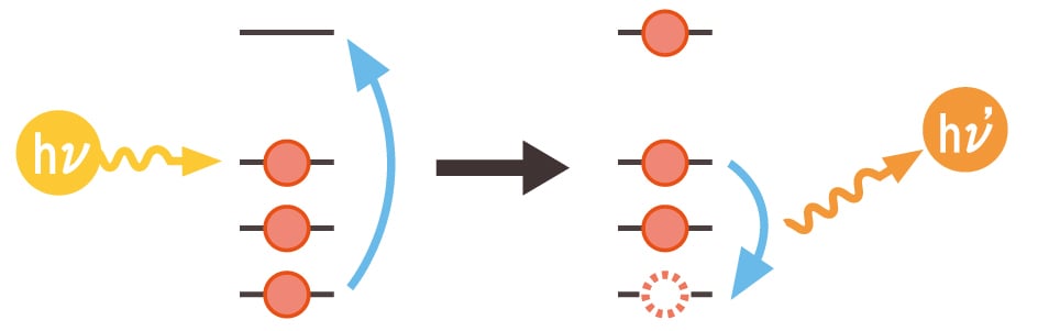
The wavelength of emitted electromagnetic waves is mainly in the X-ray region. The elements contained in the sample can be identified by irradiating the sample with an electron beam using SEM or EPMA, and at what wavelength the emitted X-ray spectrum shows the emission line.
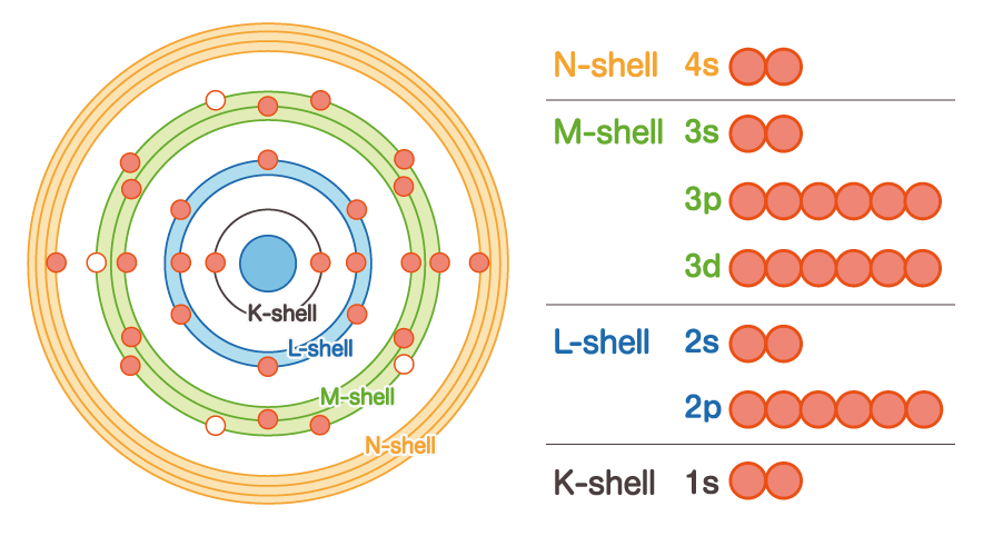
We will explain in a little more detail, including the structure of the atoms. As we learned in high school physics, atoms are made up of nuclei and electrons. And the orbits of electrons are named K-shell, L-shell, M-shell, N-shell, etc. from the inside, and to what orbits the electrons are buried depends on the element and its state. For example, the iron atom has an atomic number of 26, so there are 26 electrons including the N-shell.
By the way, the electrons in the atom will jump out of their original orbits when strong energy is given from the outside. This is called excitation. To excite an electron, it requires more energy from the inner orbit than from the outer orbit. On the other hand, the electrons come down from a higher orbit to the vacant place due to the excitation and jumping out of the electrons. At this time, the energy of the difference between the high orbit and the low orbit at the transition location is emitted as an electromagnetic wave. Names such as Kα line, Kβ line, Lα line, and Lc line are determined depending on which orbit the transition is from to which orbit.
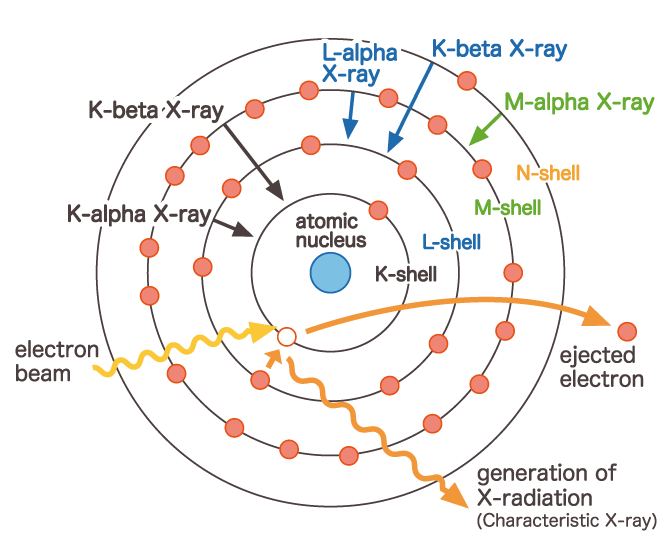
And the energy of the emitted electromagnetic wave is uniquely determined by which element and which orbit it transitioned from. Taking the energy (Kα) emitted when an electron transitions from the L-shell to the K-shell as an example, we can see that each element has its own energy value. Therefore, the wavelength of the emitted electromagnetic wave is also fixed. This X-ray is called a characteristic X-ray. By the way, when X-rays are used to excite electrons, the characteristic X-rays that are generated are called "fluorescent X-rays". In other words, when a sample is irradiated with an electron beam using SEM or EPMA, the electrons of the atoms contained in the sample are excited, and the electrons transition from a high orbit to a vacant place, emitting X-rays according to the element. By observing and analyzing this X-ray, it is possible to obtain information specific to the elements contained in the sample.
There are two main methods for analyzing characteristic X-rays. The first is called "Wavelength-dispersive X-ray spectroscopy (WDS)", which uses spectroscopic crystals to disperse characteristic X-rays and detect the decomposed wavelengths. The second is called "Energy-dispersive X-ray spectroscopy (EDS)", which uses a semiconductor detector to detect characteristic X-rays for each energy. Both methods are used for both SEM and EPMA.
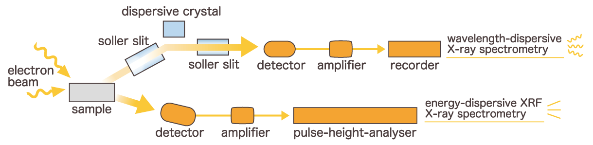
There are two types of elemental analysis methods, each of which has its strengths and weaknesses. WDS has a high energy resolution (wavelength resolution) of about 10 eV and has the advantage of being less affected by scattered X-rays and having less background noise. In addition, a microanalysis of several ppm is possible. However WDS has a narrow wavelength range that can be measured at one time and requires mechanical control to switch the spectral crystal according to the measurement wavelength, so it is not possible to identify multiple elements at once. In addition, high-precision control is required for wavelength spectroscopy using spectroscopic crystals, and the equipment tends to be large. Disadvantages include larger equipment and longer measurement times.
On the other hand, EDS uses a semiconductor detector that requires no complex moving parts for spectral acquisition, making the system compact and capable of rapid measurement. Another advantage is the ability to detect multiple elements simultaneously.
However, while performance has improved in recent years, the energy resolution is approximately 130 eV (for Mn Kα), which is lower than that of WDS, and background noise tends to be higher. Additionally, detection typically requires a concentration of at least 10 to 20 ppm. Therefore, it is important to select the appropriate method based on the analytical requirements.
By the way, EDS, which requires a small device, is mainly used in SEM. On the other hand, WDS is used in EPMA because the electron beam energy device becomes large. Of course, it is also possible to use EDS with EPMA. Compared to SEM, EPMA can be said to focus on elemental analysis.
Let's take a look at the spectrum actually obtained. The figure below is the spectrum obtained as a result of analyzing iron oxide by EDS. The horizontal axis shows the wavelength in energy (keV), and the vertical axis shows the number of detected photons (counts).
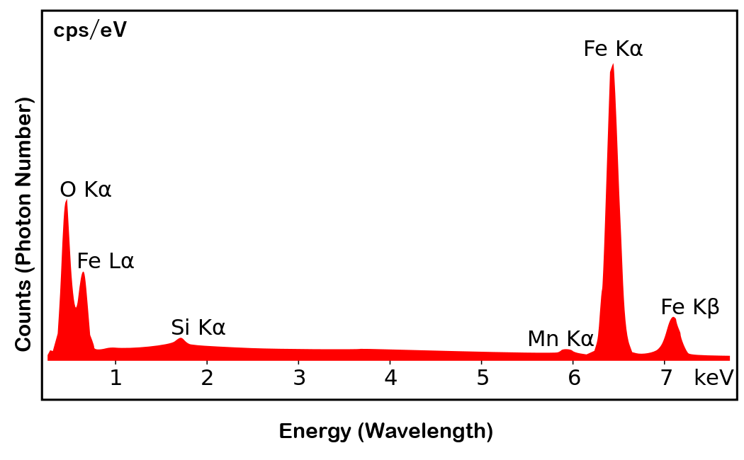
In this spectrum, iron (Fe) Kα, Kβ, and Lα are visible. You can also see that the oxygen (O) Kα is emitted. You can see that the energy (wavelength) of iron and oxygen is different for the same Kα. And you can judge that the height of the peak (more accurately, the area) indicates the concentration of the element. Therefore, the spectrum shows that the substance contains a large amount of iron and oxygen, and if this sample is an unknown sample, we can conclude that it is iron oxide. It can also be seen that this sample contains trace amounts of manganese (Mn) and silicon (Si) as impurities. In this way, it is also possible to identify how many impurities are mixed.
Other Analysis Methods
When the sample is irradiated with an electron beam by SEM or EPMA, there are some that are emitted in addition to the characteristic X-ray. One is an electron, which includes reflection electrons, secondary electrons, and Auger electrons. The other is electromagnetic waves emitted in the wavelength range of visible light. Now, let's introduce two other analysis methods using SEM and EPMA.
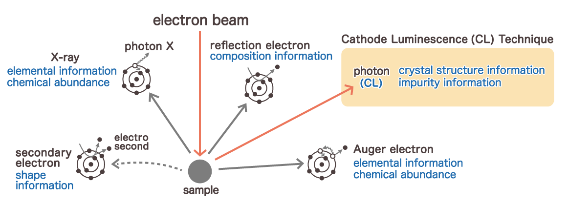
Cathode Luminescence (CL)
This method uses visible light emitted when an electron beam is applied to a sample. This light emission is called "cathodoluminescence". The method of evaluating the physical properties of a sample using this emission spectrum is called the "cathodoluminescence technique".
In the case of the cathodoluminescence technique using SEM, other signals (secondary electrons, reflection electrons, X-rays, etc.) generated by electron beams can be acquired at the same time, so it has the feature that physical properties can be evaluated in a complex manner.
The Cathodoluminescence (CL) technique investigates the crystal structure of a sample and the concentration of impurities. It is mainly used for analyzing semiconductors, dielectrics, and ceramics, aiding in the identification of crystal defects. It is also effective for measuring impurities in oxide and dielectric materials.
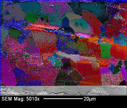
Electron Back Scattered Diffraction Pattern (EBSD)
Electron Backscatter Diffraction (EBSD) This method utilizes backscattered electrons diffracted by the crystal lattice near the sample surface to analyze crystal orientation. When a sample is tilted at 60 to 70 degrees relative to the incident electron beam, the diffracted electrons form a pattern known as a Kikuchi pattern. This pattern consists of pairs of parallel lines (Kikuchi lines) generated by diffraction from specific crystal planes.
From this pattern, the orientation of the crystal planes on the sample surface can be determined. EBSD is widely used for crystal orientation identification in microscopic regions and for generating orientation maps.
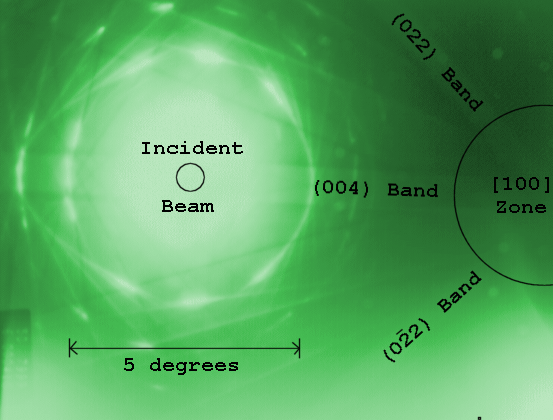
From this pattern, it is possible to investigate the orientation of the crystal plane on the sample surface. In other words, it can be used for crystal orientation identification of microscopic regions and measurement of orientation maps. If the crystal structure is not uniform and multiple microcrystals are bonded together, the crystal orientation will change depending on the location, so the direction of the Kikuchi line will also change. From this pattern, the state of the crystal can be mapped.
Related Technical Articles
Recommended products
Matsusada Precision manufactures precision high-voltage power supplies for scanning electron microscopes.


Reference (Japanese site)
- Japanese source page 「電子顕微鏡(SEM)技術解説シリーズ③ 電子顕微鏡と元素分析について」
(https://www.matsusada.co.jp/column/sem3.html) - 一般社団法人日本分析機器工業会 「X線分析法の基礎と応用」
(https://www.jaima.or.jp/jp/analytical/basic/xray/foundation) - 大阪産業技術研究所 「設備機器技術講習会[エネルギー分散型X線分析装置]」
http://tri-osaka.jp/c/content/files/archives/EDX200503.pdf (non-https address) - EBSP法の基礎原理と活用法(I)
(https://www.jstage.jst.go.jp/article/kenbikyo2004/39/2/39_2_121/_pdf) - 鳥取大学技術部 工学・情報系部門 「EPMAのしくみと試料分析例」
http://www.eng.tottori-u.ac.jp/~www_tec/epma/epma.html - 室蘭工業大学 「EPMAについて」
https://www.muroran-it.ac.jp/mat/momo/intro/epma/epma.html - 京都大学 「菊池線解析について」
http://www.tsujilab.mtl.kyoto-u.ac.jp/01TsujiLab/Education/AdvMaterDesign/2008/TextByTerada.pdf (non-https address)