
Anodic bonding is a technology used to bond silicon and glass together by applying a high voltage under elevated-temperature conditions. Because it enables excellent hermetic sealing, heat resistance, and long-term stability without the use of adhesives, it is widely utilized in high-reliability packaging for MEMS, semiconductor devices, optical instruments, and related applications.
Particularly in the MEMS field, anodic bonding has become an indispensable technology for manufacturing sensors and microfluidic devices because it allows finely fabricated silicon structures to be sealed with glass.
Anodic bonding evolved from the "Mallory Process," which was established in the 1960s. Today, in addition to conventional DC bonding, "pulse anodic bonding" is also used to reduce thermal damage and improve bonding quality.
Principle of Anodic Bonding
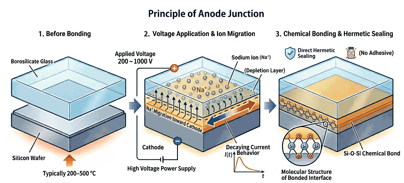
Anodic bonding is performed by heating silicon and alkali-ion-containing glass while applying a high voltage. In general, sodium-containing borosilicate glass (such as Pyrex®) and silicon wafers are heated to approximately 200-500°C, and a DC high voltage ranging from several hundred volts to several kilovolts is applied. To ensure stable bonding quality, it is important to properly match the coefficients of thermal expansion (CTE) of the silicon and glass materials.
1. Before Bonding
The borosilicate glass and silicon wafer are brought into close contact and heated.
- Mobile ions such as sodium ions (Na⁺) exist inside the glass
- Heating increases ion mobility
- No chemical bonds are formed at this stage
2. Voltage Application & Ion Migration
In general, a high voltage is applied with the silicon side serving as the anode (positive potential) and the glass side serving as the cathode (negative potential).
- Na⁺ ions inside the glass migrate toward the cathode
- A depletion layer forms at the glass-silicon interface
- A strong interfacial electric field is generated
- The strong electric field promotes intimate interface contact and facilitates the formation of Si-O-Si covalent bonds
- A relatively large current flows during the initial stage of bonding, but the current gradually decreases as ion migration progresses
This phenomenon is the fundamental principle of anodic bonding widely known as the Mallory Process.
3. Chemical Bonding & Hermetic Sealing
Once a sufficient electric field is established at the interface, Si-O-Si bonds are formed between the silicon and glass.
- Formation of Si-O-Si chemical bonds through oxygen atoms
- Direct hermetic sealing without adhesives
- High bonding strength and long-term stability
- Suitable for vacuum sealing and high-reliability packaging
Technology Trends: Pulse Anodic Bonding and ICB Technology
In recent years, pulse anodic bonding, which applies pulsed voltages to reduce thermal damage and suppress electrical discharge, has become increasingly popular.
In particular, Impulse Current Bonding (ICB) proposed by the Swiss company Sy&Se has attracted attention as a bonding technology aimed at lower-temperature processing and reduced thermal damage. Precise pulse control enables low-distortion bonding even between materials with different coefficients of thermal expansion.
This technology has already been introduced into high-end watch components and advanced MEMS manufacturing and is protected by patents. Today, major semiconductor equipment manufacturers such as SUSS MicroTec are expanding equipment offerings based on this technology, and adoption is increasing in MEMS and precision packaging applications.
Applications of Anodic Bonding
Anodic bonding enables strong bonding between silicon and glass without adhesives. Because it provides excellent hermetic sealing, superior heat resistance, and long-term stability, it is widely used in packaging processes for high-reliability MEMS and precision electronic devices.
1. Automotive MEMS Sensors
Automotive applications require long-term stable operation under harsh environments such as high temperatures, vibration, oil exposure, and humidity.
- Pressure Sensors
-
- Engine intake pressure
- Fuel pressure
- MEMS sensors for oil pressure measurement
- Accelerometers and Gyroscope Sensors
-
- Airbag deployment detection
- Electronic Stability Control (ESC)
- Vehicle attitude control
- Tire Pressure Monitoring Systems (TPMS)
-
- Highly hermetic sealing inside wheels
2. Smartphones and Consumer Electronics
Anodic bonding is widely used in MEMS packaging to achieve miniaturization and high performance.
- Electronic Compass (Magnetic Sensors)
-
- Protective sealing for micro magnetic sensor chips
- Silicon Microphones (MEMS Microphones)
-
- Protection of delicate vibration membranes
- Maintenance of acoustic performance
- Various MEMS Sensors
-
- Proximity sensors
- Pressure sensors
- Inertial sensors
3. Medical and Bio Devices
Anodic bonding is also important in fields requiring chemical stability and chemical resistance.
- Microfluidic Chips (Lab-on-a-Chip)
-
- Blood testing
- DNA analysis
- Cell analysis
- Microchannel formation
- Implantable Pressure Sensors
-
- Implantable MEMS sensors
- Ultra-small hermetic sealing
- Bio-MEMS
-
- Micropumps
- Chemical analysis devices
- Cell culture chips
4. Optical and Industrial Equipment
These applications utilize the transparency of glass and high-precision alignment capability.
- Infrared Image Sensors (Bolometers)
-
- Vacuum sealing applications
- Hermetic packaging
- Optical Switches and Projection Devices
-
- MEMS mirrors and optical switch devices
- MEMS mirror protection
- X-ray Detectors and Vacuum-Sealed Sensors
-
- Vacuum retention
- Low-outgassing sealing
- Power Semiconductor Devices
-
- High-voltage environment compatibility
- High-temperature-resistant insulation structures
5. Aerospace and Defense Applications
Anodic bonding is used to ensure long-term reliability under extreme environmental conditions.
- MEMS Sensors for Satellites
-
- Gyroscope sensors
- Accelerometers
- Vacuum-environment compatibility
- Aerospace Pressure Sensors
-
- Engine control
- Fuel control
- Defense Devices
-
- Infrared sensors
- High-durability MEMS devices
High-Voltage Power Supply Requirements for Anodic Bonding
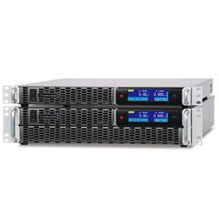
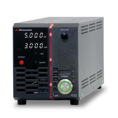
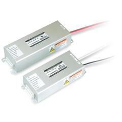
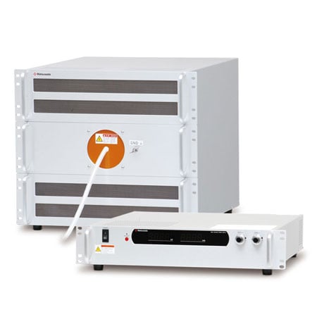
High-performance high-voltage power supplies are required in anodic bonding to stabilize bonding quality. Voltage fluctuations and abnormal discharges can cause bonding defects or damage MEMS structures, making highly stable and low-noise power performance essential.
| Item | Requirement | Purpose/Effect |
|---|---|---|
| Output Voltage | Several hundred volts to several kilovolts | Formation of a strong interfacial electric field |
| Voltage Stability | Low ripple and low noise | Stabilization of bonding quality |
| Arc Protection | Discharge detection and high-speed shutdown | Prevention of glass damage |
| Temperature Resistance | High-temperature environment compatibility | Stable operation during heating processes |
| Pulse Output Support (Pulse Bonding Only) | Compatible with pulse anodic bonding | Reduction of thermal damage |
| Response Speed (Pulse Bonding Only) | High-speed pulse response | Optimization of pulse bonding control |
| Long-Term Stability | Continuous long-duration operation | Process stabilization |
| External Control | Ethernet/RS-232C/Analog control | Automated production line compatibility |
| Safety | Interlock and insulation design | High-voltage safety measures |
In recent years, compatibility with pulse anodic bonding has become increasingly important for MEMS and wafer-level packaging applications. By utilizing high-voltage amplifiers and fast-response high-voltage power supplies, high-quality bonding can be achieved while suppressing localized heating and electrical discharge.
- Related Keywords
-
- Mallory Process
- MEMS
- Packaging
- Silicon
- Glass
- Wafer Bonding
- Hermetic Sealing
- Pulse Anodic Bonding
- Impulse Current Bonding
- ICB
- High-Voltage Power Supply
- High-Voltage Amplifier