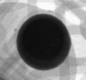
Common causes of BGA connection failures include voids, cracks, warpage, and deformation. Since the solder bumps are located beneath the chip, standard visual inspection is impossible. Furthermore, detecting these defects requires high precision, as they are often microscopic (10 μm or less). Therefore, high-resolution X-ray inspection is essential for BGA quality control.
To accurately inspect these components, the system requires a microfocus X-ray tube with a small focal spot size to minimize blur, paired with a high-resolution Flat Panel Detector (FPD). Additionally, inspecting complex BGA packages on high-layer or double-sided boards requires high tube voltage to ensure sufficient penetration through overlapping components.
The μRay8600 X-ray inspection system features a high-performance 130 kV microfocus X-ray tube and a 3-megapixel FPD, enabling clear observation at magnifications of up to 180x. The system also supports oblique viewing through its tiltable camera mechanism, allowing operators to detect bonding defects that are invisible from a direct top-down view.
| Focal Spot | Microfocus |
|---|---|
| X-ray Tube Voltage | 90 to 130 kV |
| Magnification | 100x or more |